Incident: +3V3 Split Plane — the regulator feeds nothing
Date: 2026-07-25 · Severity: Critical (no boot, no display power) · Affected: all PCB v1 — design bug · Related: C2 reversed · Power short
TL;DR
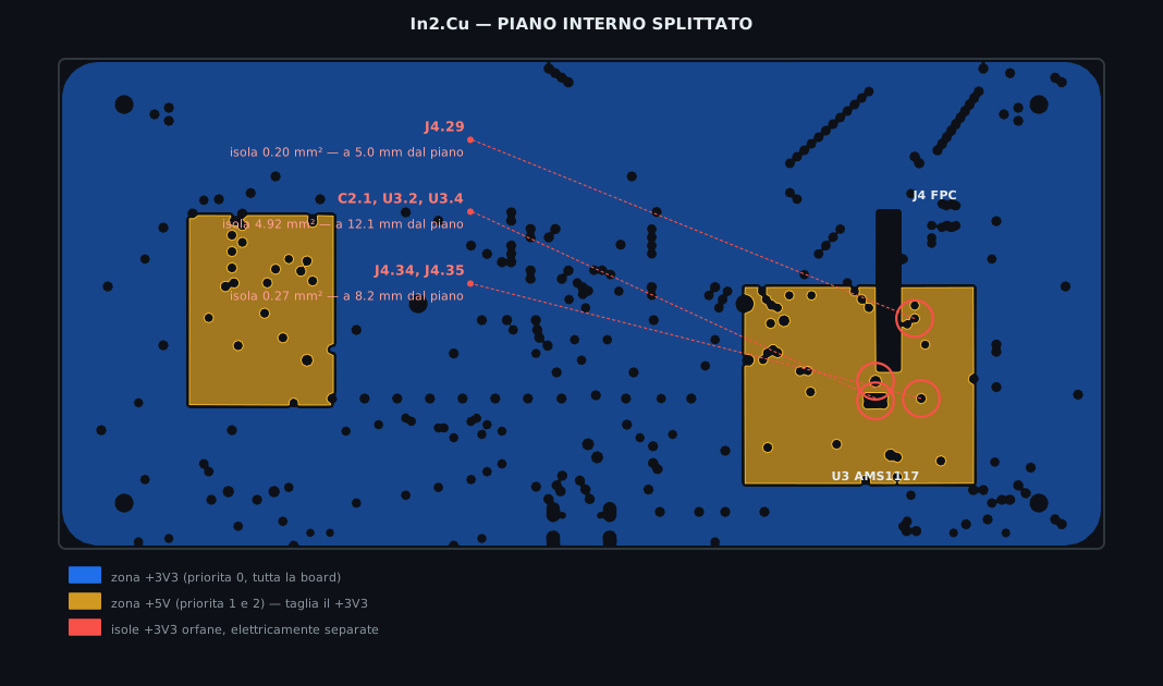
The AMS1117 outputs a clean 3.3 V that reaches nothing. On In2.Cu the
+3V3 copper is split into four separate groups: the regulator sits on a
4.92 mm² orphan island, 12.1 mm from the main plane that feeds the ESP32,
display, SD and all button pull-ups. No short — an open, which is why the
thermal camera shows nothing: no load, no current, no heat. Cold is the
signature of an open.
Root cause
In2.Cu is a split plane: the board-wide +3V3 zone has priority 0, and two
+5V zones sit on top at priority 1 and 2. U3 lands at (125, 55.5) — inside
the priority-1 rectangle, which ate the +3V3 copper around the regulator
output. Three of the display's supply pins (J4.29/.34/.35 — panel VDD/VDDI)
ended on their own orphan islands the same way.
Control on the same board with the same detector: GND → 1 group, +5V → 1
group. Only +3V3 was broken; the method does not produce false positives.
Why the checks did not catch it
KiCad DRC was reporting it — as 7 unconnected_zone items baselined in
drc_baseline.json under the assumption "power nets connect through
inner-layer zones". The zone that was supposed to connect them was the thing
that was split. And verify_net_connectivity.py, written for exactly this
failure mode, skipped GND/+3V3/+5V by default because it could not parse
poured polygons. The one script that would have found the bug excluded the
three nets it happened on.
Every one of those suppressions is now deleted: the baseline buckets are gone,
drc_native.py exits 1 on real issues, and power nets are checked against the
real poured geometry by default. See the project rule: never silence errors.
Rework (both jumpers mandatory)

- Jumper 1 — power the board: AWG26 minimum (the whole board's current
flows through it) from
U3pad 4 (the SOT-223 tab, (125.00, 52.35)) toC4pad 1 ((92.95, 42.00), the ESP32 decoupling cap). The tempting 14.6 mm via at (141.06, 61.72) is buried under the SD socket — unreachable. - Jumper 2 — power the display: bridge
J4.29,J4.34,J4.35(0.5 mm pitch, work under magnification) toJ4.3on the main plane. - Bring-up: continuity U3.4 → U1.2 → J4.3 → J4.35;
+3V3↔GND not 0 Ω; current-limited supply 200 mA, idle < 50 mA; 3.3 V measured atC4.1, not at the regulator.
Note for future probing: FPC numbering is connector_pad = 41 − panel_pin by
design; connector pads 9–16, 27, 28, 33, 37–40 legitimately carry no net.
Panel pin 40 reading continuity to GND is IM2 strapping, not a fault.
The regression guard
make verify-power-nets (verify_power_net_integrity.py): +3V3/+5V/GND/VBUS/
BAT+ must each be one geometric group — no allowlist, and a power net
with no copper fails rather than passing vacuously. The detector
(pcb_copper_graph.py) is the single implementation shared by the gate, the
connectivity check and the figure renderer, and over-approximates copper so it
can only merge groups, never split them: a reported split is never a
geometric false positive. Mutation-tested by test_power_net_integrity.py;
runs inside verify-all, release-prep and the Stop hook.
The un-suppressed run also surfaced VBUS in 4 groups (two known USB-C reverse-orientation pads, plus a zero-length B.Cu segment nobody had ever listed) — hidden by the same baseline buckets.
v2 fix
Raise +3V3 zone priority above the +5V zones, reshape the priority-1
rectangle so it does not enclose U3, or route the regulator output with
explicit copper. verify-power-nets stays red until one lands — the gate is
the acceptance test.