PCB Design — JLCPCB PCBA
Custom 4-layer PCB designed for fabrication and assembly by JLCPCB. Maximum components assembled on-board to minimize manual soldering.
Interactive BOM Viewer — click components to highlight on PCB layout
PCB Renders
3D Raytraced Renders
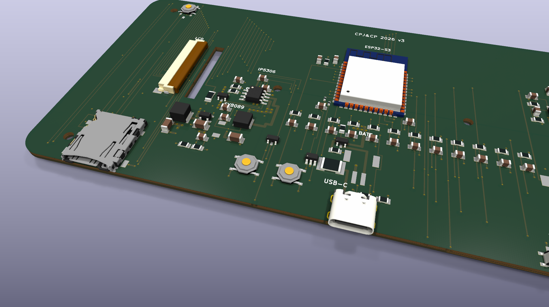
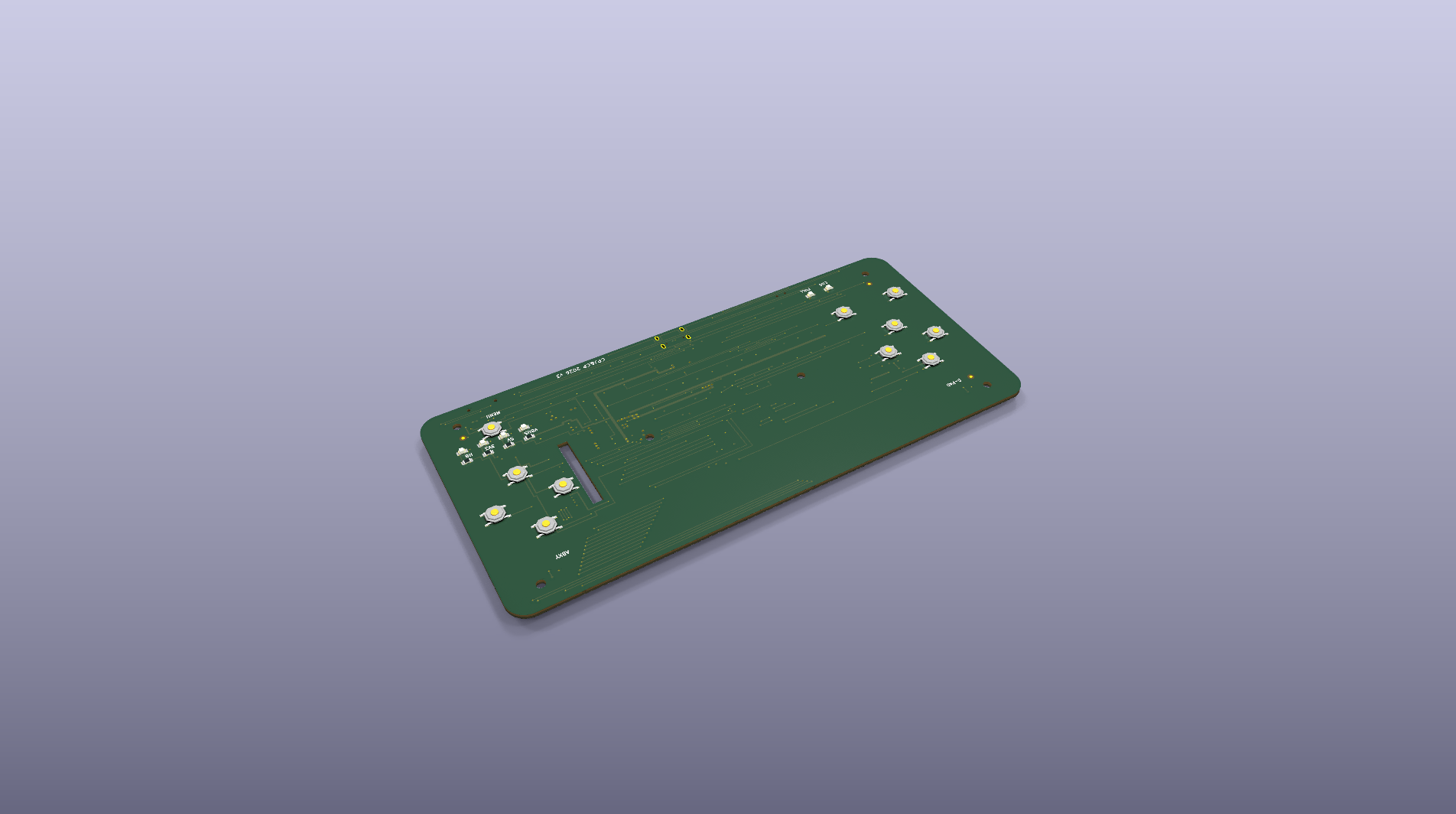
Photorealistic renders generated by KiCad 10 raytracer with 3D component models.
| Top Side (F.Cu) | Bottom Side (B.Cu) |
|---|---|
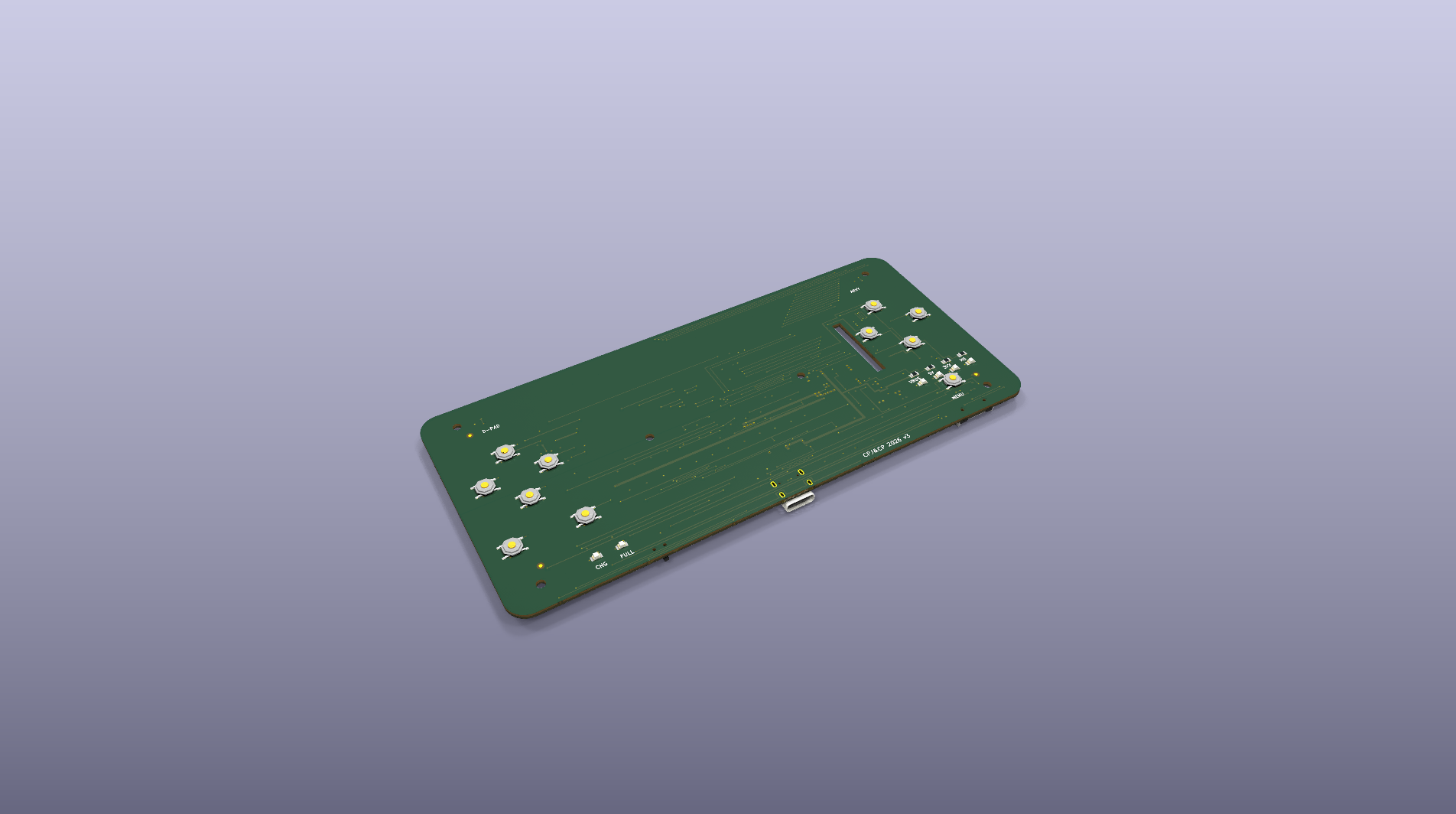 | 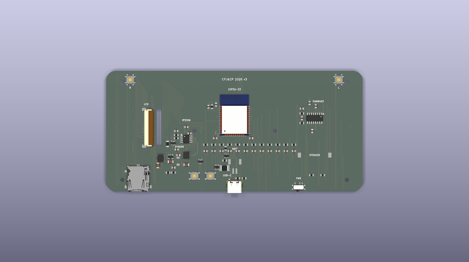 |
| Isometric Front | Isometric Back |
|---|---|
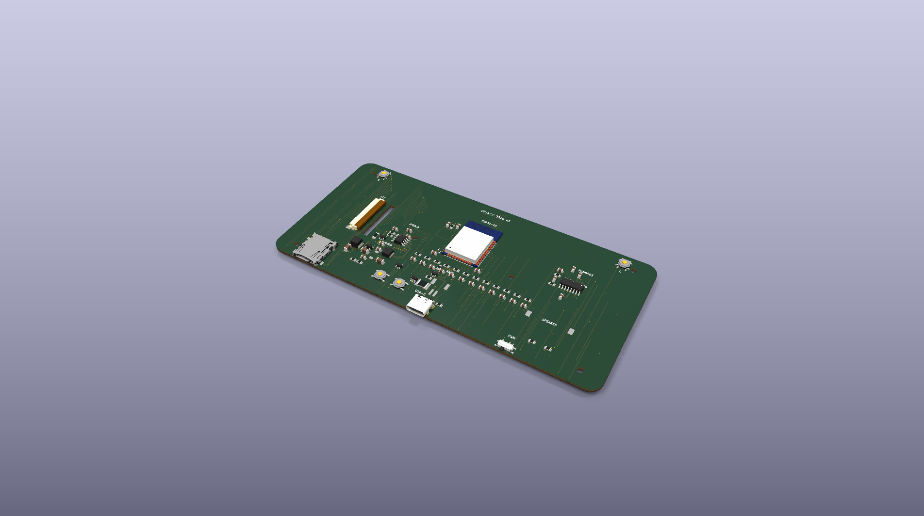 | 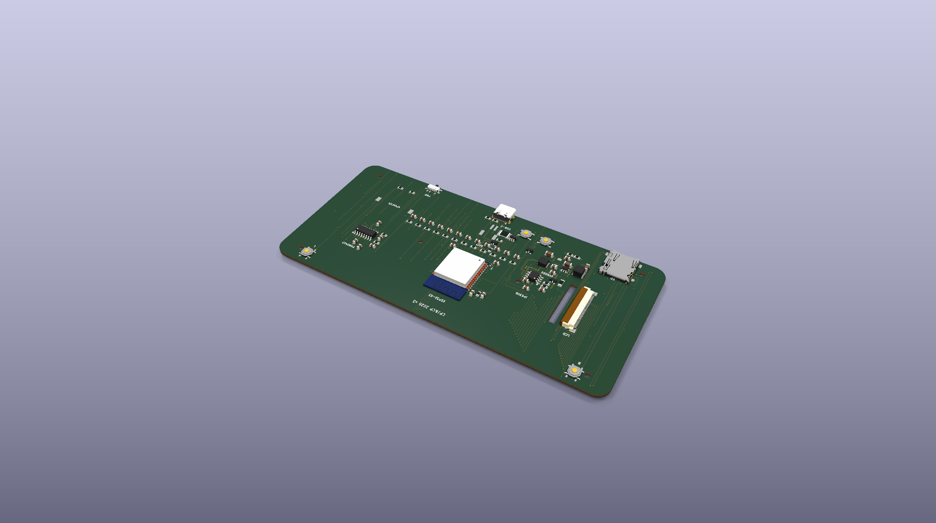 |
| ESP32 Detail | Bottom Isometric |
|---|---|
 |  |
Interactive 3D Viewer
Open interactive 3D PCB viewer — rotate, zoom, explode view, top/bottom toggle.
Board Specifications
| Parameter | Value |
|---|---|
| Dimensions | 160 × 75 mm |
| Layers | 4 (F.Cu, In1.Cu GND, In2.Cu Power, B.Cu) |
| Thickness | 1.6 mm |
| Surface Finish | ENIG (gold) |
| Corner Radius | 6 mm |
| FPC Slot | 3 × 24 mm vertical cutout (40-pin ribbon pass-through) |
| Mounting Holes | 6× M2.5 — the 4 corner holes land on the enclosure's screw bosses; the 2 centre holes are PCB-only (the enclosure's centre bosses were removed because they fouled the battery) |
Layer Stackup
| Layer | Function |
|---|---|
| F.Cu (Top) | Face buttons, menu button, charging LEDs |
| In1.Cu | Full GND copper pour |
| In2.Cu | +3V3 / +5V power plane |
| B.Cu (Bottom) | ESP32, ICs, connectors, passives, L/R shoulder buttons |
Component Placement
Top Side (F.Cu) — User-facing
- 11× SMT tact switches — D-pad (left), ABXY (right), Start/Select
- SW13 Menu button — bottom right
- LED1, LED2 — charging indicators (bottom left)
- ILI9488 3.95" bare LCD panel sits on top (FPC ribbon passes through slot to J4 on back)
FPC Slot & Pin Reversal
- 3 × 24 mm vertical cutout between display area and ABXY buttons
- Allows the 40-pin FPC ribbon cable to pass from top (display) to bottom (J4 connector)
- Located at x=127mm from left edge, vertically centered with display
- Pin reversal: the display in landscape (CCW rotation) has Pin 1 at the south end of the FPC tail. The cable passes straight through the slot without twisting, so display Pin N contacts connector Pad (41−N). All PCB traces account for this reversal.
Bottom Side (B.Cu) — Electronics
- SW11, SW12 — L/R shoulder buttons (top edge, rotated 90°)
- U1 ESP32-S3-WROOM-1 — center
- U2 IP5306 (eSOP-8) — charger + boost, left-center area
- U3 SY8089AAAC (SOT-23-5) — 3.3V synchronous buck, below center, with L2/C1/C30 kept in a tight switching loop
- U5 PAM8403 (SOP-16) — audio amp, left area
- L1 1µH inductor — near IP5306
- J1 USB-C — bottom center
- U6 Micro SD slot — bottom right (VCC/GND connect via vias to inner power planes)
- J4 FPC 40-pin 0.5mm — right of FPC slot (display ribbon, ILI9488)
- J3 JST PH 2-pin — battery connector, center
- SW16 — power slide switch (MSK12C02), left edge — drives Q2's gate, carries no rail current
- Q2 (SOT-23, 118.20/45.00, rot 90) — SW16 respin high-side P-MOSFET, splits
+5V_VOUTfrom+5V - R32/R33/R34, C32, C33 — Q2 gate network + IP5306 KEY wake cap (IP5306 quadrant)
- SW17 — TS-1088 land for the manual KEY wake button (DO NOT PLACE — in BOM, absent from CPL)
- SPK1 — solder pads for the 28 mm speaker (footprint
Speaker-28mm: two 2×3 mm wire pads, 19 mm apart), left area - C21-C25, R20-R21 — PAM8403 passives (near U5)
- 26× passives — organized in 2 centered rows below ESP32
Bill of Materials (BOM)
JLCPCB-Assembled Components
38 line items, 99 BOM placements (98 fitted — SW17 is DO NOT PLACE). The authoritative table is generated from
release_jlcpcb/bom.csv — the exact file uploaded to JLCPCB — and lives on the
BOM page. It is
regenerated by make docs-bom and make docs-bom-check fails the build when it
drifts, so it is never hand-edited. The headline parts:
| Ref | Component | LCSC | Qty |
|---|---|---|---|
| U1 | ESP32-S3-WROOM-1-N16R8 | C2913202 | 1 |
| U2 | IP5306 charger+boost | C181692 | 1 |
| U3 | SY8089AAAC 2A buck | C78988 | 1 |
| U4 | USBLC6-2SC6 USB ESD TVS | C7519 | 1 |
| U5 | PAM8403 audio amp | C5122557 | 1 |
| U6 | Micro SD slot (TF-01A) | C91145 | 1 |
| J1 | USB-C 16-pin | C2765186 | 1 |
| J3 | JST PH 2-pin SMD (battery) | C295747 | 1 |
| J4 | FPC 40-pin 0.5mm (display) | C2856812 | 1 |
| L1 / L2 | 1µH boost / 2.2µH buck inductor | C280579 / C36409 | 1 each |
| Q1, Q2 | AO3401A P-MOSFET (Q1 battery RPP, Q2 +5V load switch) | C15127 | 2 |
| D1 / F1 | Menu-combo Schottky / VBUS PTC | C37704 / C960026 | 1 each |
| LED1, LED2 | Red LED 0805 (both are plain +3V3 power indicators) | C84256, C19171391 | 2 |
| SW1–SW17 | 15× SMT tact switch + 1× slide switch (MSK12C02) + 1× TS-1088 (DNP) | C318884, C431540, C720477 | 17 |
Three references sit on the board but are not assembled: R14 (DNP by
design — BTN_L must have no external pull-up), C28 (unused placeholder) and
SW17 (manual KEY wake, in the BOM so it can be sourced but absent from the
CPL). SPK1 is a pad pair for the hand-soldered speaker, and FID1–FID3 are
fiducials. That is 98 placed + 7 non-placed = 105 references on the board.
Manual Assembly — Buy Separately
These components are NOT provided by JLCPCB and must be purchased from AliExpress (see BOM):
| Component | Buy | Connection | Soldering |
|---|---|---|---|
| LiPo 3.7V 5000mAh (105080) | ~$6-8 | Plug into JST PH connector (J3) | No — plug-in connector |
| ILI9488 3.95" bare LCD panel (40P FPC, touch NC) | ~$3.95 | Insert 40-pin FPC ribbon into J4 connector, close latch | No — plug-in FPC |
| 28mm 8Ω speaker | ~$0.80 | Solder 2 wires to pads on PCB | Yes — 2 solder points |
| — | Removed — GPIOs reassigned to USB data and BTN_R | — |
Buy the bare LCD panel (NOT a module with PCB breakout):
- ILI9488 3.95" 320×480, 40-pin FPC 0.5mm pitch
- Resistive touch (not connected on PCB)
- AliExpress
- The FPC ribbon slides into J4 and locks — zero soldering.
JLCPCB Ordering
Files Needed
All production files are pre-packaged in the release_jlcpcb/ folder at the project root:
- Gerber ZIP —
release_jlcpcb/gerbers.zip(ready to upload, inner layers with zone fill) - BOM.csv —
release_jlcpcb/bom.csv(38 part-number groups, 99 designators) - CPL.csv —
release_jlcpcb/cpl.csv(98 component placements — SW17 is BOM-only, DO NOT PLACE)
Order Settings
- Layers: 4
- PCB Qty: 5
- Thickness: 1.6mm
- Surface Finish: ENIG
- Assembly: Both sides
- Tooling holes: Added by JLCPCB
Estimated Cost (5 boards)
Real quote for the shipped design (5 units, both sides assembled):
| Item | Cost |
|---|---|
| PCB fabrication (4-layer) | $31.50 |
| PCBA assembly + fees | $166.36 |
| Total | $197.86 (~$39.57/board) |
Most of that is one-time setup (engineering, stencil, feeders, fixture ≈ $106.73), so the per-unit cost falls steeply with quantity. Full line-by-line breakdown: PCBA Manufacturing & Ordering.
Schematic Architecture
The design uses a hierarchical schematic with a root file referencing 6 sub-sheets:
| Sheet | File | Components |
|---|---|---|
| Root | esp32-emu-turbo.kicad_sch | 6 sheet references |
| 1 | 01-power-supply.kicad_sch | USB-C, IP5306, SY8089 buck, battery, LEDs, power switch, USB data + ESD (U4, R22/R23) |
| 2 | 02-mcu.kicad_sch | ESP32-S3 + decoupling + EN reset RC |
| 3 | 03-display.kicad_sch | ILI9488 bare panel + FPC 40-pin connector (J4) |
| 4 | 04-audio.kicad_sch | PAM8403 + speaker (SPK1) |
| 5 | 05-sd-card.kicad_sch | Micro SD SPI interface |
| 6 | 06-controls.kicad_sch | 13 buttons + pull-ups + debounce caps |
There is no 07-usb-data.kicad_sch — the native USB path is drawn on Sheets 1
and 2 and joined by the USB_D+/USB_D- global labels (see
USB Data).
Total: 91 component references on the board, 85 assembled by JLCPCB.
Generation
# Generate schematics (6 sheets + root)
python3 -m scripts.generate_schematics hardware/kicad

# Generate PCB + JLCPCB exports
make generate-pcb

# Render PCB images
make render-pcb

# Verify schematic/PCB/JLCPCB consistency
python3 scripts/verify_schematic_pcb.py
Output files:
hardware/kicad/esp32-emu-turbo.kicad_sch— Hierarchical root schematichardware/kicad/01-06-*.kicad_sch— 6 sub-sheet schematicshardware/kicad/esp32-emu-turbo.kicad_pcb— KiCad PCB layouthardware/kicad/jlcpcb/cpl.csv— Component Placement List (85 parts)
Routing Architecture
All traces use Manhattan (orthogonal) routing — horizontal segments on F.Cu, vertical segments on B.Cu, with vias at every direction change.
Trace Widths
| Category | Width | Nets |
|---|---|---|
| Power high | 0.76mm | VBUS, BAT+, LX (up to 2.1A) |
| Power | 0.60mm | +5V, +3V3, GND returns |
| Power low | 0.30mm | +3V3/GND short cap-to-via stubs (~0.5A) |
| Audio | 0.30mm | PAM8403 → speaker |
| Signal | 0.25mm | Buttons, passives |
| Data | 0.20mm | Display bus, SPI, I2S, USB |
SPI Bus Routing (v1.3 fix)
SD_MOSI and SD_MISO originally ran as long horizontal traces on F.Cu (~45mm, from ESP32 to SD card), crossing the FPC approach zone where LCD data bus and button traces also run on F.Cu. This caused 3 trace shorts:
| Short | Cause |
|---|---|
| SD_MOSI (y=32.58) ↔ LCD_D4 (y=32.75) | Parallel traces within 0.2mm on F.Cu |
| SD_MOSI (y=32.58) ↔ BTN_Y (y=32.5) | Parallel traces within 0.2mm on F.Cu |
| SD_MISO (y=33.85) ↔ LCD_D6 (y=33.75) | Parallel traces within 0.2mm on F.Cu |
Fix: SD_MOSI and SD_MISO now use B.Cu vertical bypass columns at x=120 and x=118 respectively. The traces drop to B.Cu before the conflict zone, run vertically to the SD card y-level, then continue on F.Cu to the SD card pins. SD_CLK and SD_CS were unaffected and use the direct route.
Inner Layer Power Planes
| Layer | Net | Coverage | Zone Priority |
|---|---|---|---|
| In1.Cu | GND | Full board | 0 |
| In2.Cu | +3V3 | Full board (base) | 0 |
| In2.Cu | +5V | Center-right (105-123, 35-62) | 1 |
| In2.Cu | +5V | PAM8403 area (20-39.6, 24-53) | 2 |
| In2.Cu | +5V_VOUT | IP5306 corner (105-120.3, 35-45) | 3 (highest) |
The +5V islands on In2.Cu cover the SY8089/L1 area and the PAM8403 corner; since the SW16 respin the IP5306 end of that region is carved out as +5V_VOUT at priority 3 — the boost-output net upstream of Q2. Higher priority wins in each overlap, and components outside these areas connect to +3V3 via the base zone.
This exact arrangement cut the +3V3 zone into four electrically separate groups and left the regulator on a 4.92 mm² orphan island — no v1 board ever had 3.3 V at the ESP32. See the incident. make verify-power-nets now fails when any power net resolves to more than one copper group.
The Python PCB generator creates zone boundaries but does not fill them — zone fill requires the KiCad pcbnew API. The make export-gerbers pipeline runs kicad_fill_zones.py via Docker before exporting Gerber files, ensuring inner layers contain full copper pour data.
Pre-Production Verification
All automated checks passed before the JLCPCB production order:
Short Circuit Analysis — PASS
| Check | Result |
|---|---|
| Trace Shorts | ✅ PASS (0 shorts) |
| Zone Fill Data | ✅ PASS (7 filled polygons) |
| Zone Priorities | ✅ PASS |
| Gerber File Sizes | ✅ PASS (In1_Cu=243KB, In2_Cu=260KB) |
Script: python3 scripts/short_circuit_analysis.py
DRC (Design Rule Check) — PASS
| Rule | JLCPCB Min | Our Design | Status |
|---|---|---|---|
| Trace width | 0.09mm | 0.2mm (data), 0.6mm (power) | PASS |
| Trace spacing | 0.09mm | 0.2mm | PASS |
| Via drill | 0.15mm | 0.2mm | PASS |
| Via pad | 0.35mm | 0.35–0.46mm | PASS |
| Annular ring | 0.075mm | 0.075–0.13mm | PASS |
| Board edge clearance | 0.3mm | 0.5mm | PASS |
DRC Engine: KiCad native DRC with JLCPCB custom rules (hardware/kicad/esp32-emu-turbo.kicad_dru)
Script: python3 scripts/drc_native.py --run (zone fill + DRC + smart analysis)
Electrical Simulation — PASS (6 warnings)
Power Budget:
- +3V3 rail: 335mA max / 800mA capacity (42% utilization)
- +5V rail: 387mA max / 2.4A capacity (16% utilization)
- SY8089 buck thermal: ~0.07W typical / ~0.12W peak (was 0.57W with the AMS1117 LDO)
- Battery life: ~12.9 h typical on the 5000 mAh cell — derived through both conversion stages in Power Budget
Signal Timing:
- Display 8080 bus: 18.4 MB/s required, 20 MB/s available (8% margin)
- SPI SD card: 6MB ROM loads in 1.3s
- I2S audio: 32kHz SNES rate, BCLK 1.024MHz (ESP32 max 8MHz)
- Button debounce: RC = 1.0ms (acceptable range 1-10ms)
Component Values:
- USB-C CC pull-down: R1,R2 = 5.1kΩ (USB-C spec: 4.7k-5.6k) ✓
- LED current: 1.1-1.3mA (safe, visible) ✓
- Pull-up logic: 3.3V > Vih 2.475V ✓
- Decoupling caps present near all ICs ✓
GPIO Mapping:
- 31 GPIOs used, no conflicts with the module's flash (GPIO 26-32) or Octal PSRAM (GPIO 33-37)
- Strapping pins documented (GPIO0, GPIO3, GPIO45, GPIO46)
- GPIO19/20 used for native USB data (D-/D+); GPIO43 reassigned from TX0 to SD_MISO; GPIO3 reassigned to BTN_R
Script: python3 scripts/simulate_circuit.py
Schematic/PCB Consistency — PASS
- All 85 JLCPCB CPL components matched between schematic, PCB, and CPL
- Off-board symbols excluded: battery (BT1) and the display panel (DS1) — both connect by cable
- PCB: 664 trace segments, 341 vias, 57 nets, 91 footprints (+6 mounting holes)
Script: python3 scripts/verify_schematic_pcb.py
Run All Verifications
# All checks in one command
make verify-all

# Or individually:
python3 scripts/drc_native.py --run       # JLCPCB DRC with smart analysis
python3 scripts/simulate_circuit.py       # Electrical verification
python3 scripts/verify_schematic_pcb.py   # Schematic/PCB consistency
python3 scripts/short_circuit_analysis.py # Short circuits + zone fill

# Export Gerbers with zone fill (requires Docker)
make export-gerbers
DRC Improvements (Feb 2026):
- Integrated JLCPCB custom
.kicad_drurules (4-layer, standard vias) - Smart violation categorization (known-acceptable vs real issues)
- Baseline tracking for delta detection (regression prevention)
- Source file mapping with fix suggestions for real issues
- Reduced critical violations from 186 → 10 borderline clearance issues (0.032-0.085mm vs 0.09mm JLCPCB min)
- Fixed 8 unconnected items in power routing (VBUS, +5V, +3V3, BAT+, LX nets)
v2 PCB — Audio Coprocessor
The v2 revision adds an ESP32-S3-MINI-1-N8 audio coprocessor to the bottom side of the PCB. See Phase 5 — Software Architecture for the full rationale.
v2 Component Placement
| Ref | Component | Side | Location | Notes |
|---|---|---|---|---|
| U7 | ESP32-S3-MINI-1-N8 | B.Cu (bottom) | Near PAM8403 (left area) | SPI slave + I2S output |
| C34,C35 | 100nF 0805 | B.Cu (bottom) | Adjacent to U7 | Decoupling (C1–C33 are taken on v1 — C32/C33 are the SW16 respin's gate and wake caps) |
v2 Routing Changes
| Connection | v1 | v2 |
|---|---|---|
| GPIO 15 (main ESP32) | unused (I2S_BCLK reservation retired — PDM needs only DOUT) | SPI_CLK → U7 (MINI-1) |
| GPIO 16 (main ESP32) | unused (I2S_LRCK reservation retired) | SPI_MOSI → U7 (MINI-1) |
| GPIO 17 (main ESP32) | I2S_DOUT → PAM8403 | SPI_MISO ← U7 (MINI-1) |
| GPIO 20 (main ESP32) | USB_D+ (native USB) | SPI_CS → U7 (MINI-1) |
| U7 GPIO 15 | — | I2S_BCLK → PAM8403 |
| U7 GPIO 16 | — | I2S_LRCLK → PAM8403 |
| U7 GPIO 17 | — | I2S_DOUT → PAM8403 |
The PAM8403 audio amplifier input changes from the main ESP32-S3 to the MINI-1 coprocessor. The I2S bus traces from U7 to U5 (PAM8403) are short and direct since both are on the bottom side in the left area.
v2 Schematic Architecture
| Sheet | File | Components |
|---|---|---|
| Root | esp32-emu-turbo.kicad_sch | 7 sheet references |
| 1–6 | (same as v1) | (same as v1) |
| 7 | 07-audio-coprocessor.kicad_sch | ESP32-S3-MINI-1-N8 + decoupling |
v2 Total: 94 component references on the board, 88 assembled by JLCPCB.
Next Steps
v1 (current)
- Upload
release_jlcpcb/gerbers.zipto jlcpcb.com - Upload
release_jlcpcb/bom.csvandrelease_jlcpcb/cpl.csvfor SMT assembly - Order 5× PCBs with SMT assembly (98 placements)
- Buy off-board components: bare LCD panel (40P FPC), LiPo battery, speaker (see table above)
- Manual assembly: plug battery into J3, insert 40-pin FPC into J4, solder speaker wires
v2 (audio coprocessor)
- Add ESP32-S3-MINI-1-N8 to KiCad schematic (Sheet 8) and PCB layout
- Re-route I2S traces from U7 to U5 (PAM8403), SPI traces from U1 to U7
- Re-export Gerbers, BOM, and CPL for JLCPCB
- Order v2 PCBs with 88 assembled components
- Flash coprocessor firmware via separate USB connection or SPI bootloader