PCB v2.9 — Visual Rework Guide
Complete visual guide for all 27 routing violations found on the production PCB v2.9 (tag v2.9, commit adc073b). Each fix includes an annotated PCB render showing the exact location, the problem, and the rework procedure.
Source: hardware/debug/all-shorts-rework.md
Tools needed: soldering iron (fine tip), flux, 30AWG kynar wire, precision knife, multimeter, loupe or microscope.
Summary
| Severity | Count | Description | Fixes |
|---|---|---|---|
| CRITICAL | 3 | Power-to-power bridge (GND↔VBUS, GND↔+5V) | FIX 1-3 |
| HIGH | 5 | Signal bridges two power nets (+3V3↔GND) | FIX 4-8 |
| MEDIUM-HIGH | 19 | Signal touches one power net | FIX 9-27 |
Rework priority: perform the fixes in numerical order. Test with a multimeter after each one.
FIX 1-3: Power Shorts (CRITICAL)
These shorts prevent the board from powering on. FRONT side (F.Cu, display).
FIX 1 — VBUS → GND via
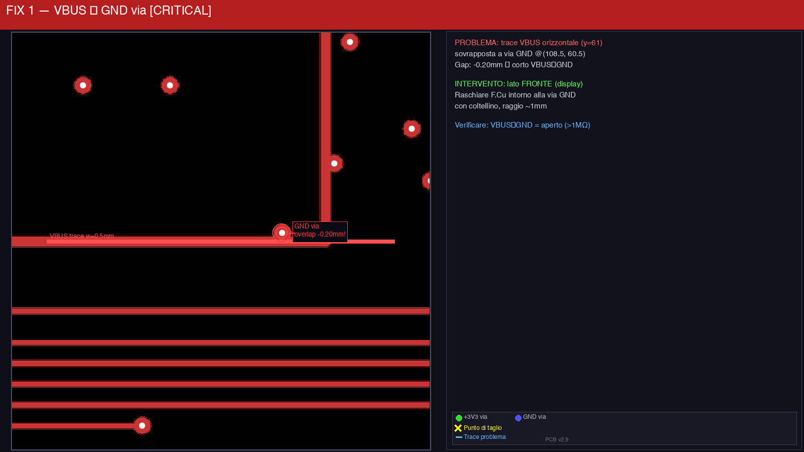
| Detail | |
|---|---|
| Layer | F.Cu (front) |
| Trace | VBUS horizontal (y=61, w=0.5mm) |
| Via | GND @ (108.5, 60.5) ø0.9mm |
| Gap | -0.20mm |
| Effect | VBUS shorted to GND → board does not power on |
| Action | Scrape the F.Cu around the GND via (~1mm radius) |
| Verify | Multimeter: VBUS↔GND = open (>1MΩ) |
FIX 2 — VBUS → +5V via
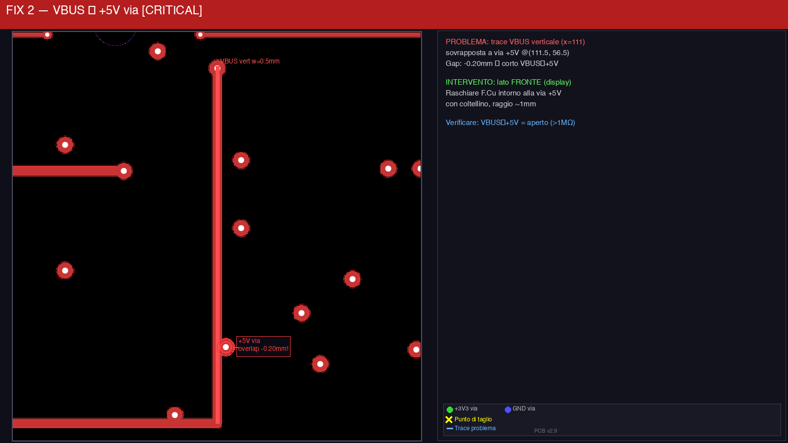
| Detail | |
|---|---|
| Layer | F.Cu (front) |
| Trace | VBUS vertical (x=111, w=0.5mm) |
| Via | +5V @ (111.5, 56.5) ø0.9mm |
| Gap | -0.20mm |
| Effect | VBUS shorted to +5V |
| Action | Scrape the F.Cu around the +5V via (~1mm radius) |
| Verify | Multimeter: VBUS↔+5V = open (>1MΩ) |
FIX 3 — LCD_RST bridges VBUS↔GND
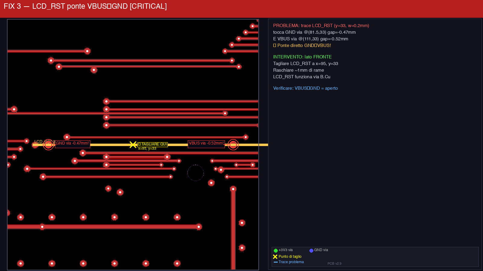
| Detail | |
|---|---|
| Layer | F.Cu (front) |
| Trace | LCD_RST horizontal (y=33, w=0.2mm) |
| Via 1 | GND @ (81.5, 33) — gap: -0.47mm |
| Via 2 | VBUS @ (111, 33) — gap: -0.52mm |
| Effect | Direct GND↔VBUS bridge through the LCD_RST copper |
| Action | Cut the LCD_RST trace at x=95, y=33. Scrape ~1mm. LCD_RST still works through its B.Cu route. |
| Verify | Multimeter: VBUS↔GND = open (>1MΩ) |
FIX 4-8: Signal Bridges +3V3↔GND (HIGH)
Vertical B.Cu traces that cross both a +3V3 via and a GND via, creating power-to-power bridges. BACK side (B.Cu, components). 4 cuts per fix.
FIX 4 — USB_D- bridges +3V3↔GND
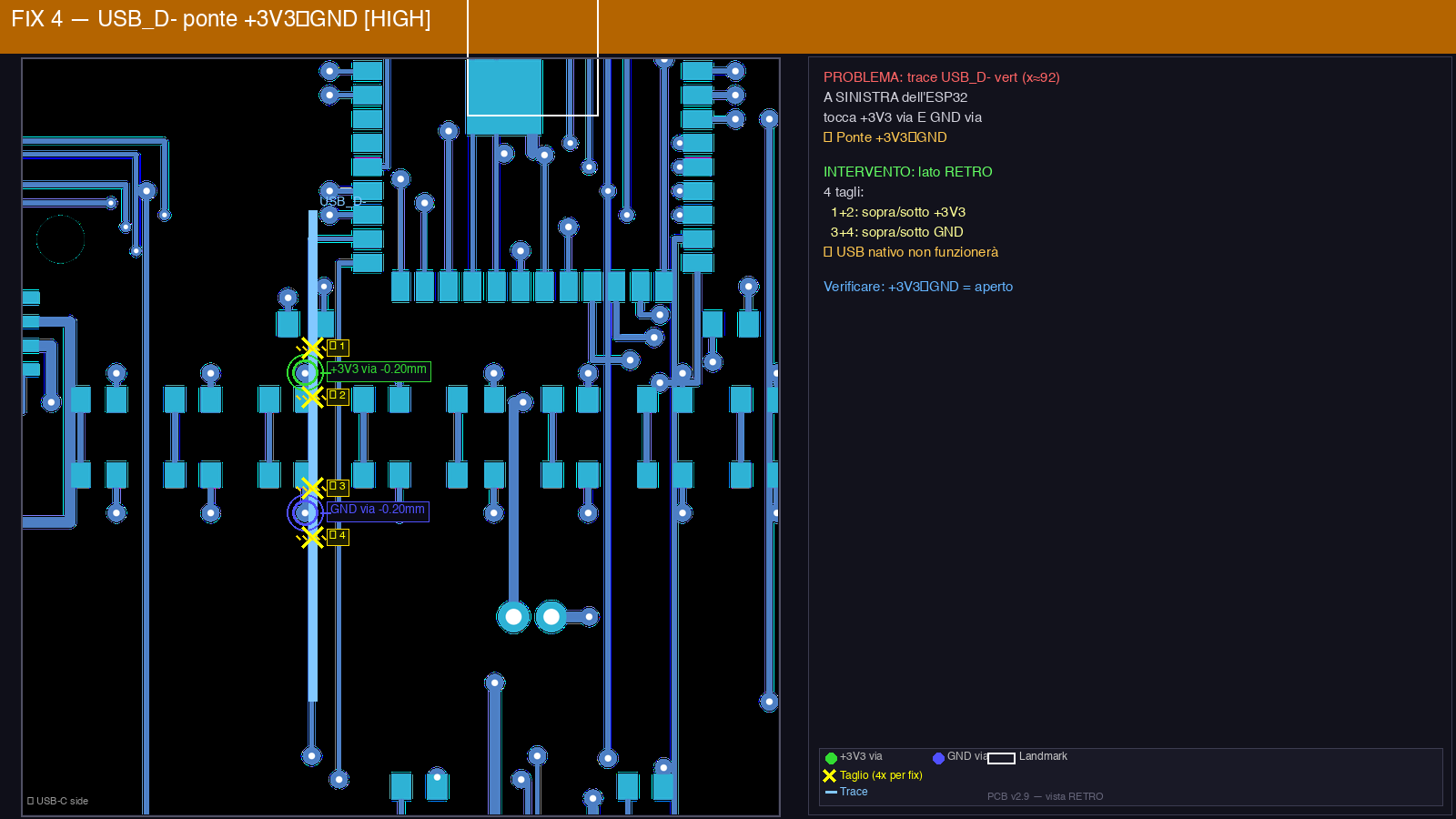
| Detail | |
|---|---|
| Layer | B.Cu (back) |
| Trace | USB_D- vertical (x=91.7, w=0.2mm) |
| Via 1 | +3V3 @ (92.05, 44.6) — gap: -0.20mm |
| Via 2 | GND @ (92.05, 52.0) — gap: -0.20mm |
| Effect | +3V3↔GND bridge through the USB_D- copper |
| Action | 4 knife cuts: above and below each via. ⚠ Native USB will stop working. |
| Verify | Multimeter: +3V3↔GND = open (>1MΩ) |
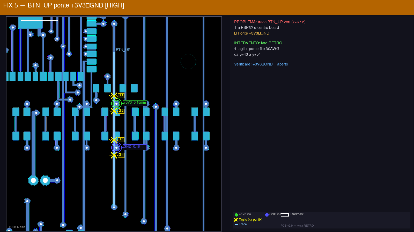
FIX 5 — BTN_UP bridges +3V3↔GND
| Detail | |
|---|---|
| Layer | B.Cu (back) |
| Trace | BTN_UP vertical (x=67.5, w=0.25mm) |
| Via 1 | +3V3 @ (67.05, 44.6) — gap: -0.18mm |
| Via 2 | GND @ (67.05, 52.0) — gap: -0.18mm |
| Action | 4 cuts + a 30AWG wire jumper from y=43 to y=54 |
| Verify | +3V3↔GND = open |
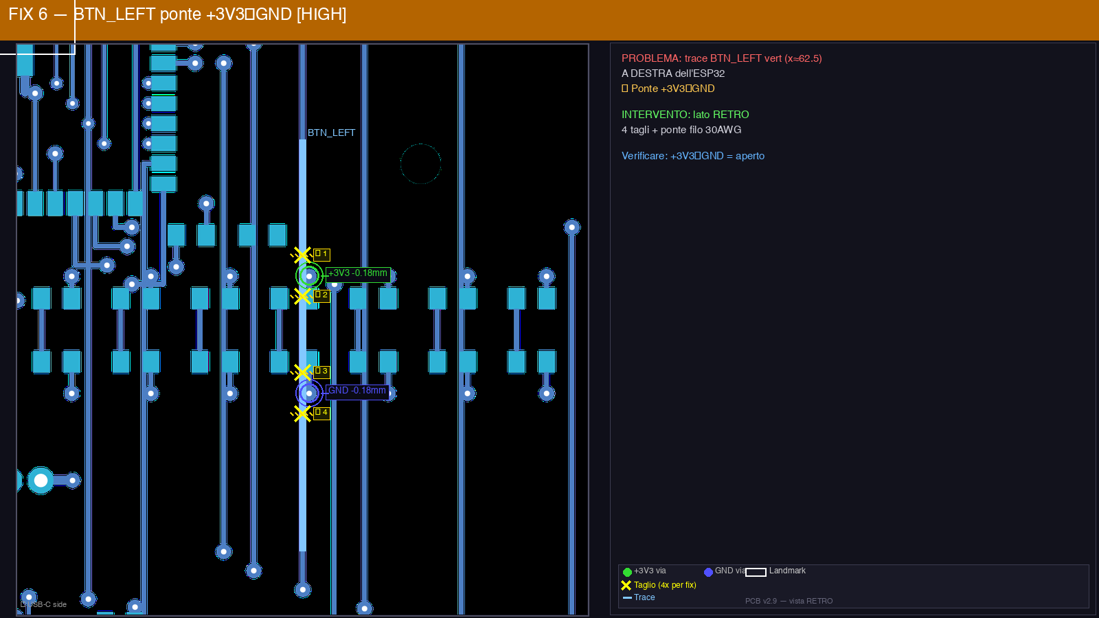
FIX 6 — BTN_LEFT bridges +3V3↔GND
| Detail | |
|---|---|
| Layer | B.Cu (back) |
| Trace | BTN_LEFT vertical (x=62.5, w=0.25mm) |
| Via 1 | +3V3 @ (62.05, 44.6) — gap: -0.18mm |
| Via 2 | GND @ (62.05, 52.0) — gap: -0.18mm |
| Action | 4 cuts + 30AWG wire jumper |
| Verify | +3V3↔GND = open |
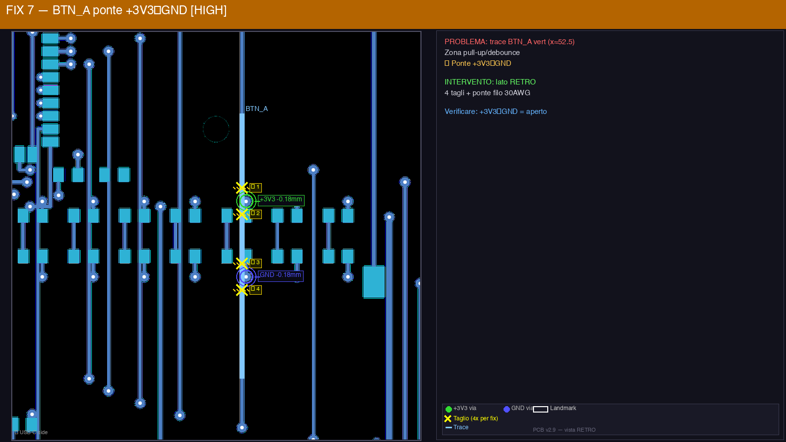
FIX 7 — BTN_A bridges +3V3↔GND
| Detail | |
|---|---|
| Layer | B.Cu (back) |
| Trace | BTN_A vertical (x=52.5, w=0.25mm) |
| Via 1 | +3V3 @ (52.05, 44.6) — gap: -0.18mm |
| Via 2 | GND @ (52.05, 52.0) — gap: -0.18mm |
| Action | 4 cuts + 30AWG wire jumper |
| Verify | +3V3↔GND = open |
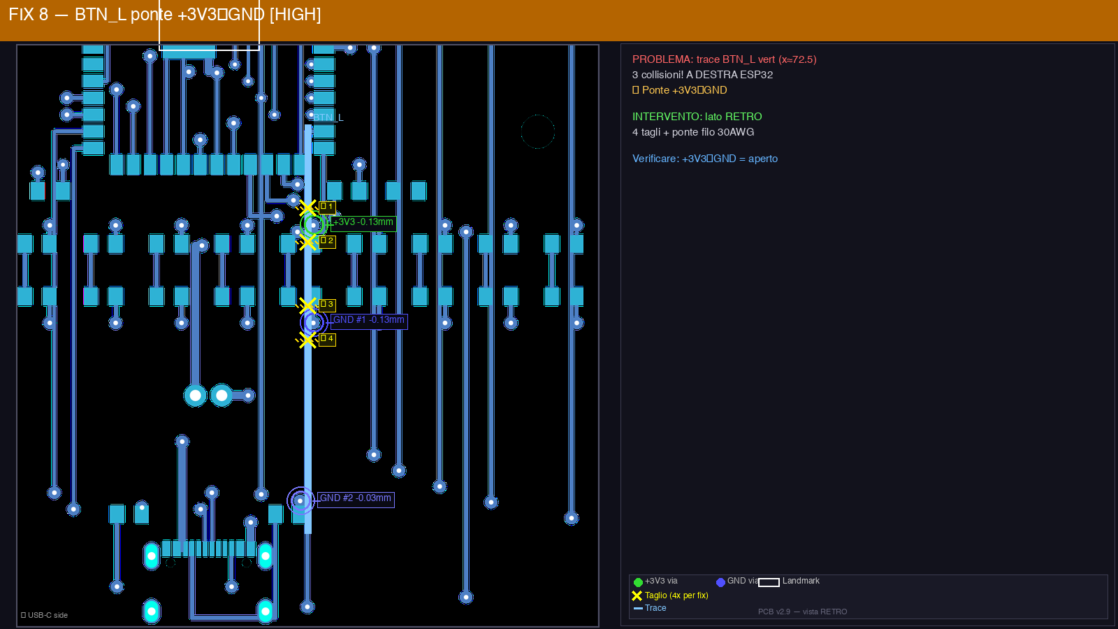
FIX 8 — BTN_L bridges +3V3↔GND
| Detail | |
|---|---|
| Layer | B.Cu (back) |
| Trace | BTN_L vertical (x=72.5, w=0.25mm) |
| Via 1 | +3V3 @ (72.05, 44.6) — gap: -0.13mm |
| Via 2 | GND @ (72.05, 52.0) — gap: -0.13mm |
| Via 3 | GND @ (73.05, 65.5) — gap: -0.03mm |
| Action | 4 cuts on the 2 main vias + a 30AWG wire jumper |
| Verify | +3V3↔GND = open |
FIX 9-27: Single-Net Shorts (MEDIUM)
A signal trace touching ONE power via. This creates no power-to-power bridge, but it clamps the signal to that power net's level. Action: scrape the copper around the via (~1mm radius).
FIX 9 — BTN_Y → +3V3 (F.Cu)
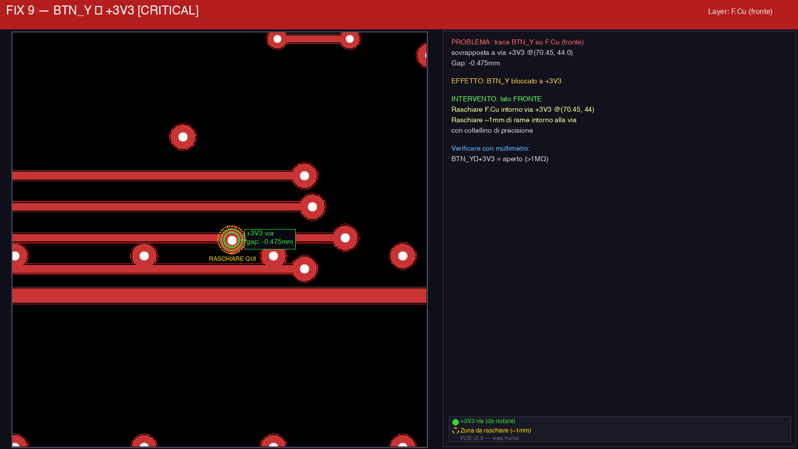
| Trace | Via | Gap | Effect | Fix |
|---|---|---|---|---|
| BTN_Y | +3V3 @ (70.45, 44.0) | -0.475mm | BTN_Y stuck HIGH | Scrape the F.Cu around the via |
FIX 10 — USB_D+ → GND (F.Cu)
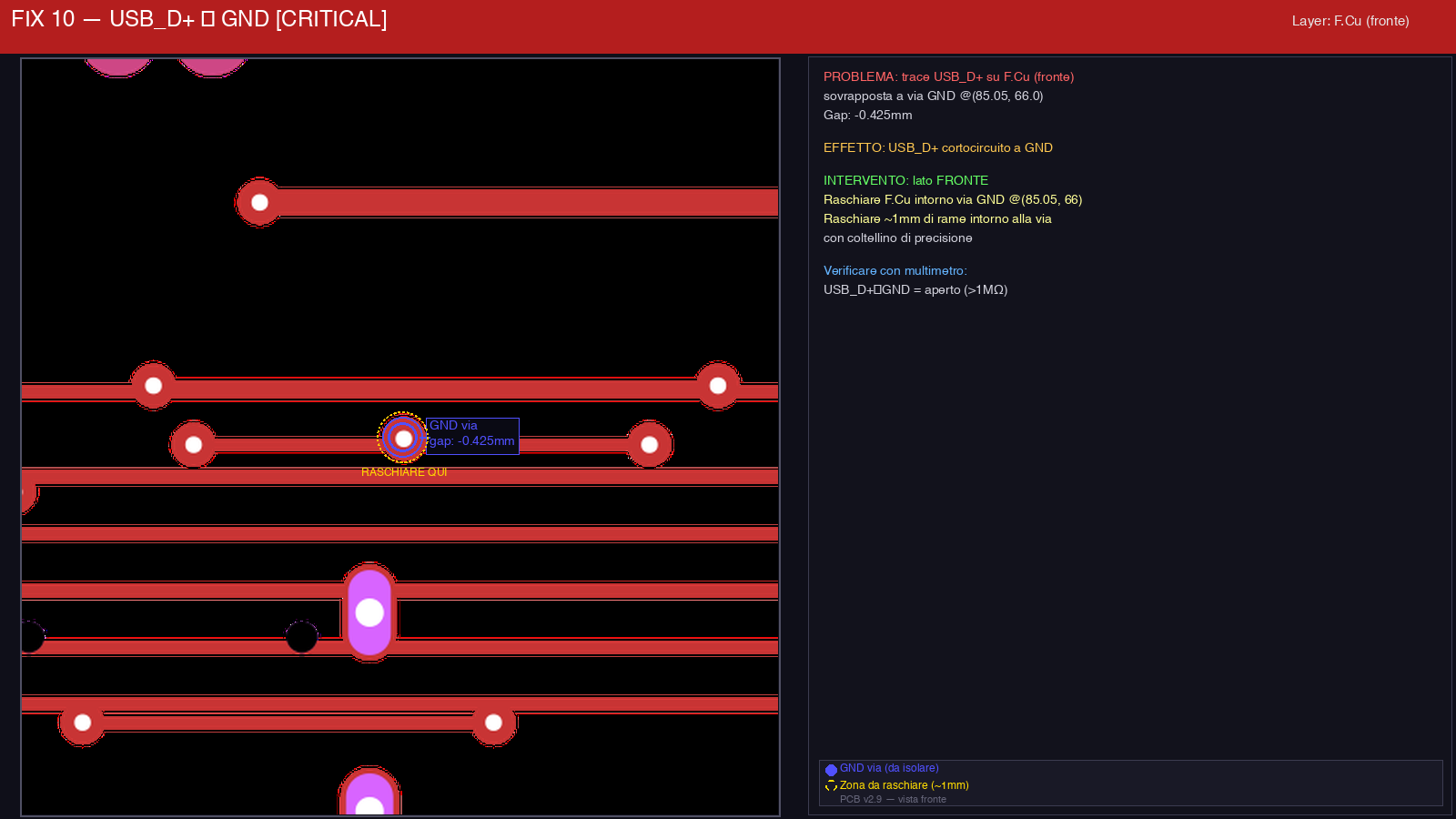
| Trace | Via | Gap | Effect | Fix |
|---|---|---|---|---|
| USB_D+ | GND @ (85.05, 66.0) | -0.425mm | USB_D+ shorted to GND | Scrape the F.Cu around the via |
FIX 11 — LCD_DC → GND (F.Cu)
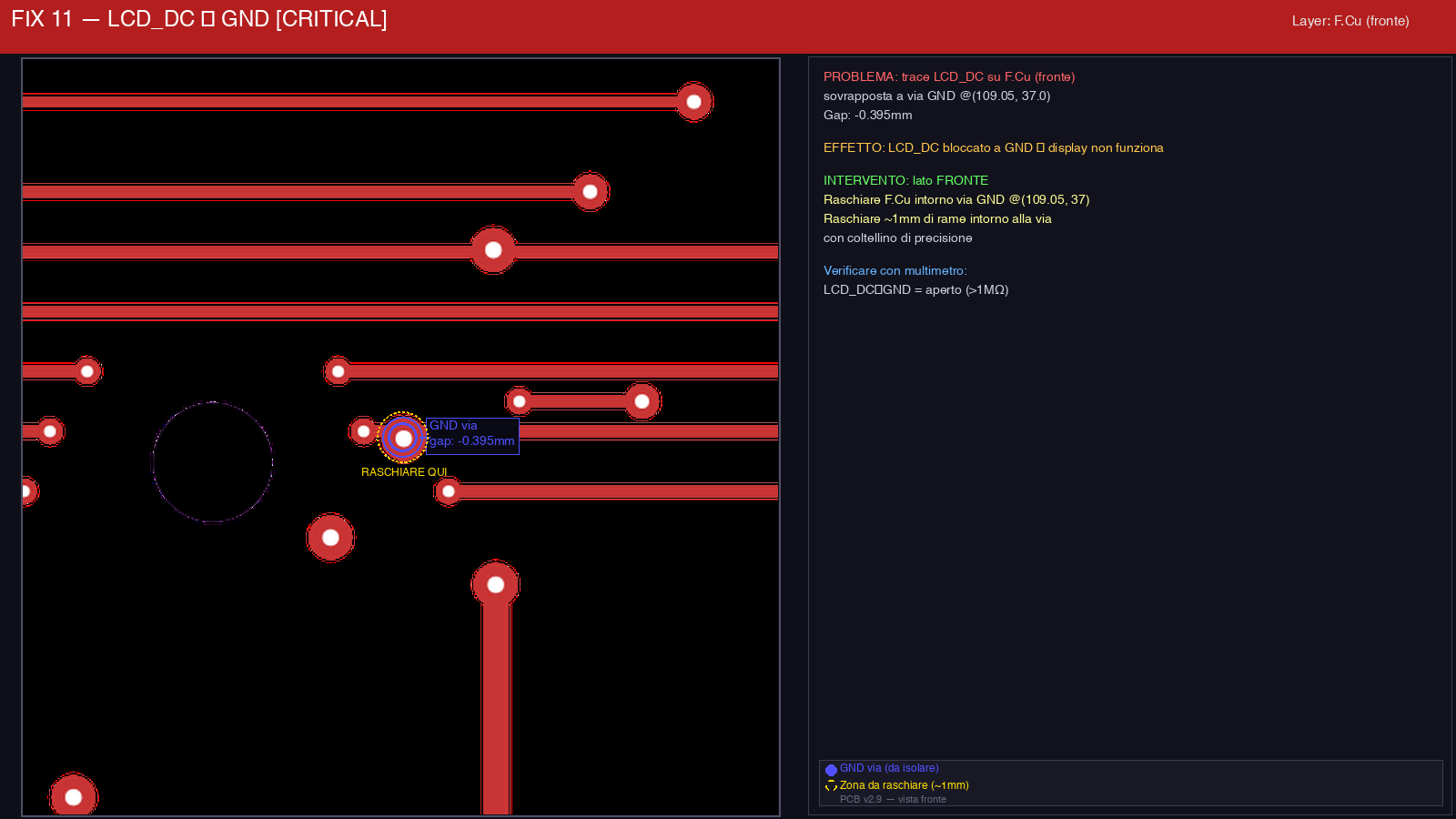
| Trace | Via | Gap | Effect | Fix |
|---|---|---|---|---|
| LCD_DC | GND @ (109.05, 37.0) | -0.395mm | Display does not work | Scrape the F.Cu around the via |
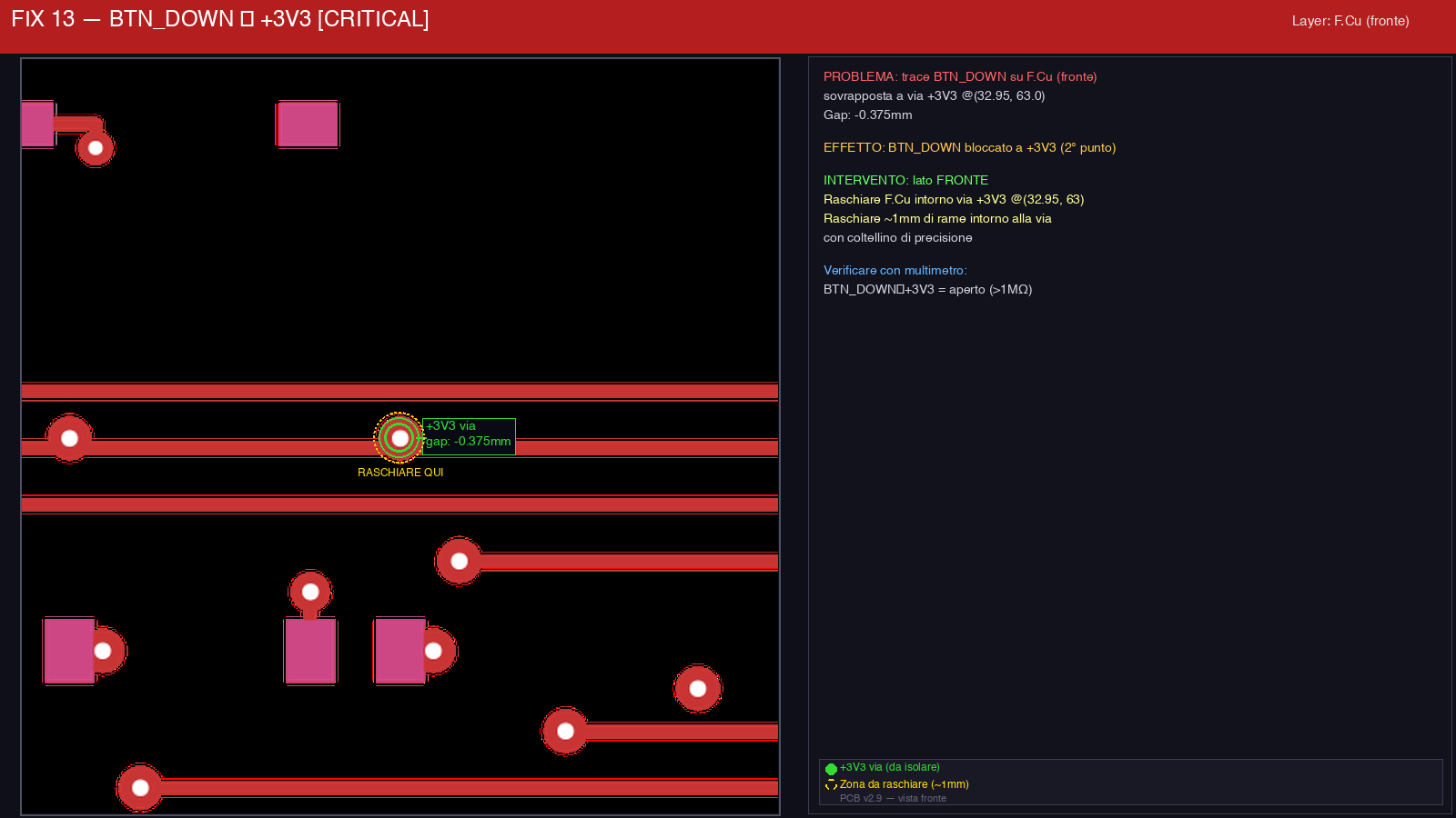
FIX 12-13 — BTN_DOWN → +3V3 (F.Cu, 2 spots)
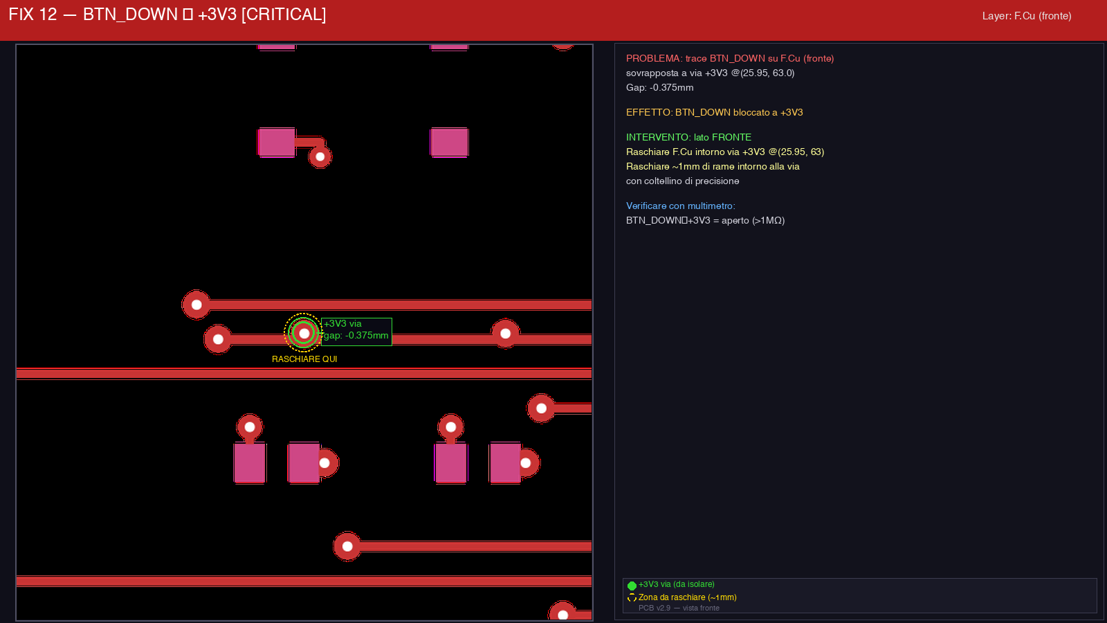
| # | Via | Gap | Fix |
|---|---|---|---|
| 12 | +3V3 @ (25.95, 63.0) | -0.375mm | Scrape the F.Cu |
| 13 | +3V3 @ (32.95, 63.0) | -0.375mm | Scrape the F.Cu |
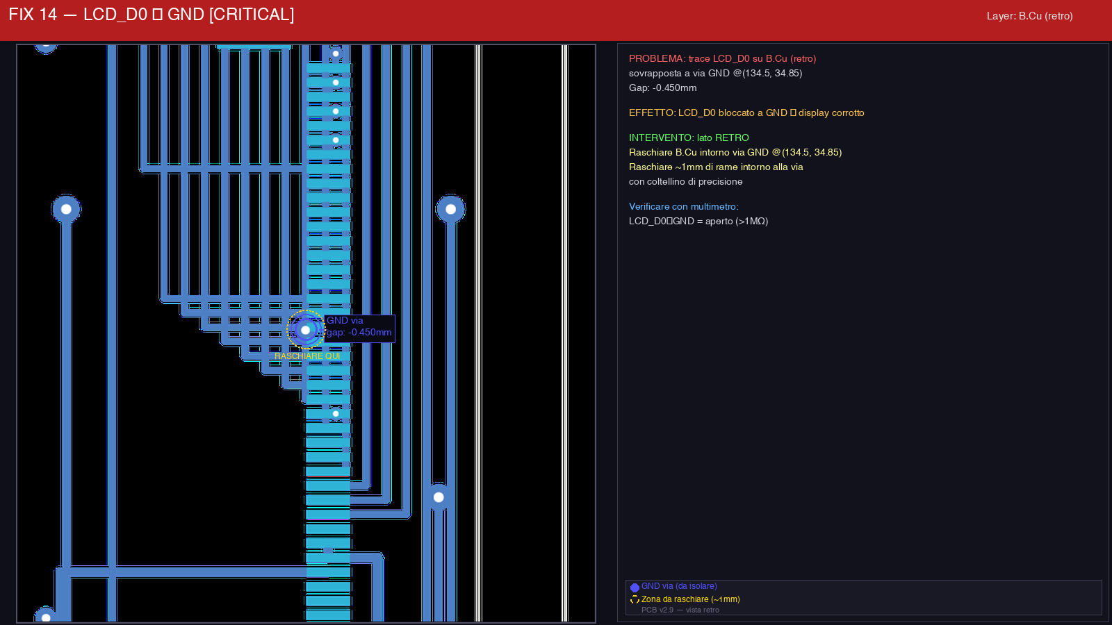
FIX 14, 16, 25 — LCD_D0/D5/D4 → GND (B.Cu, same via)
| # | Signal | Via | Gap |
|---|---|---|---|
| 14 | LCD_D0 | GND @ (134.5, 34.85) | -0.450mm |
| 16 | LCD_D5 | GND @ (134.5, 34.85) | -0.350mm |
| 25 | LCD_D4 | GND @ (134.5, 34.85) | -0.050mm |
Single action: scraping the B.Cu around the GND via @ (134.5, 34.85) resolves all three.
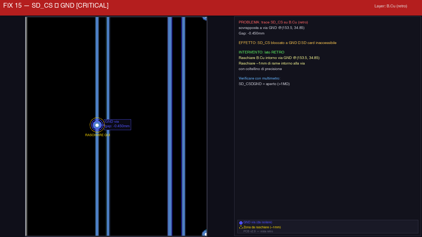
FIX 15 — SD_CS → GND (B.Cu)
| Trace | Via | Gap | Effect | Fix |
|---|---|---|---|---|
| SD_CS | GND @ (153.5, 34.85) | -0.450mm | SD card unreachable | Scrape the B.Cu around the via |
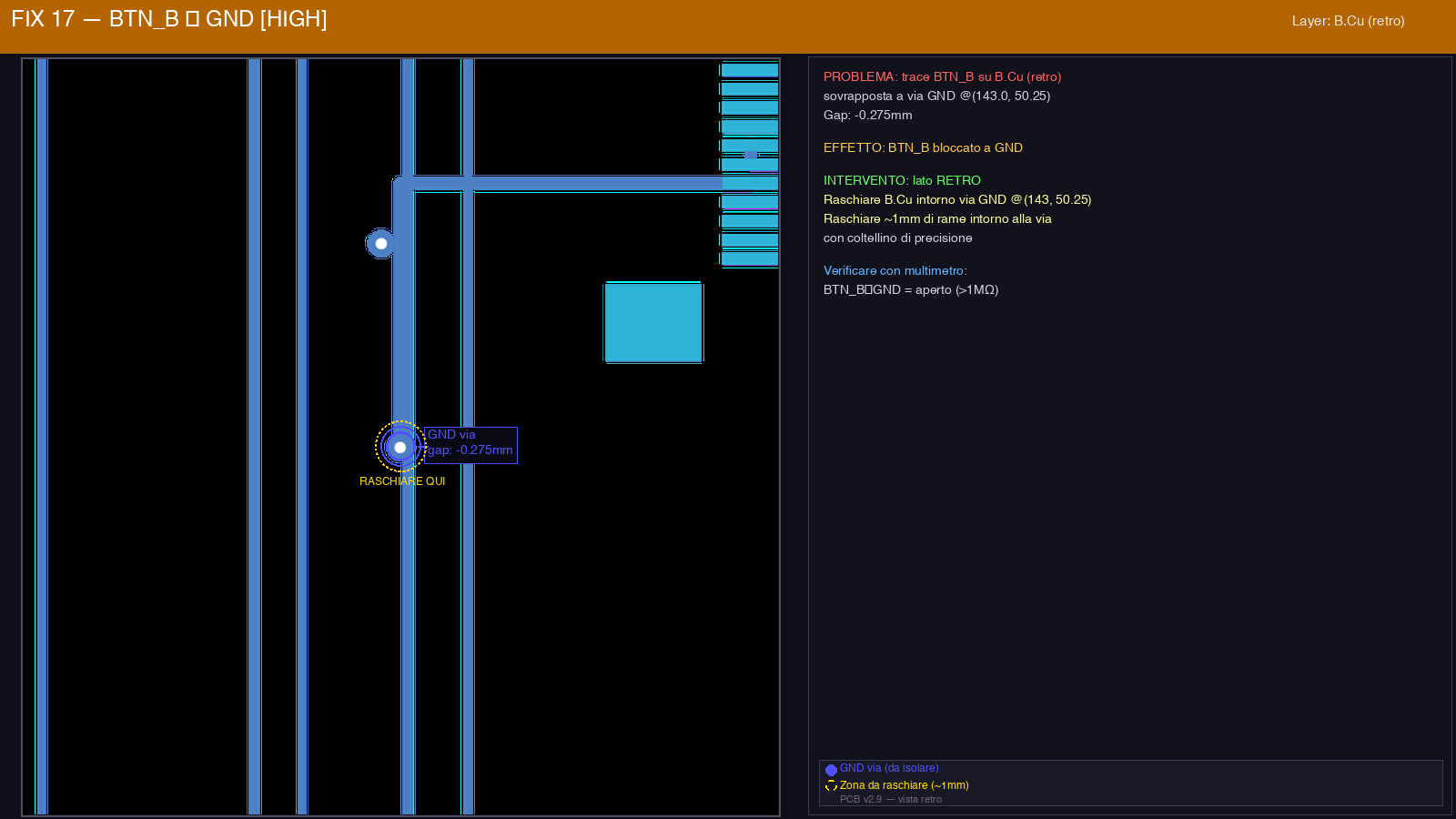
FIX 17 — BTN_B → GND (B.Cu)
| Trace | Via | Gap | Effect | Fix |
|---|---|---|---|---|
| BTN_B | GND @ (143.0, 50.25) | -0.275mm | BTN_B stuck LOW | Scrape the B.Cu around the via |
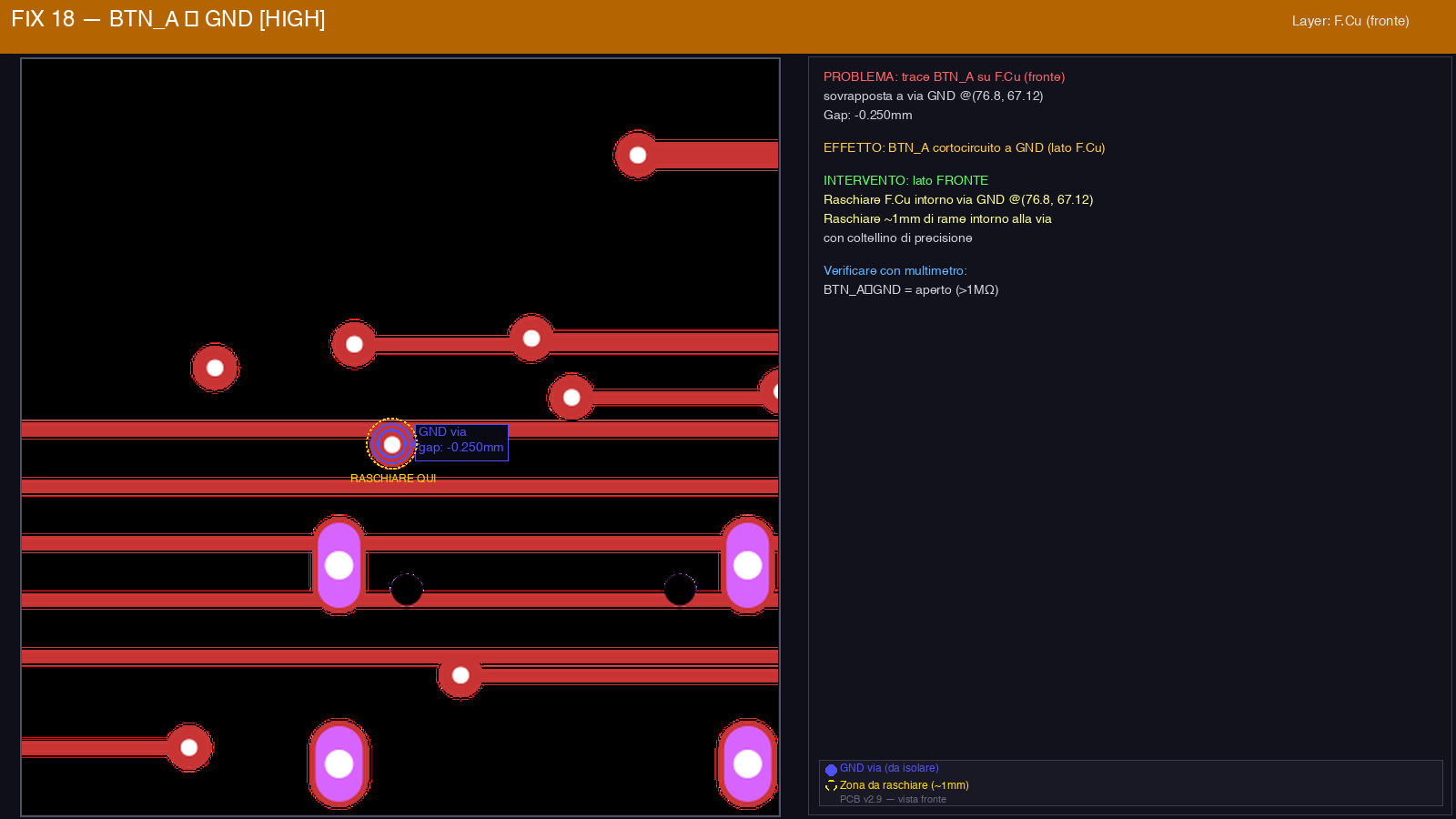
FIX 18 — BTN_A → GND (F.Cu)
| Trace | Via | Gap | Effect | Fix |
|---|---|---|---|---|
| BTN_A | GND @ (76.8, 67.12) | -0.250mm | BTN_A shorted to GND | Scrape the F.Cu around the via |
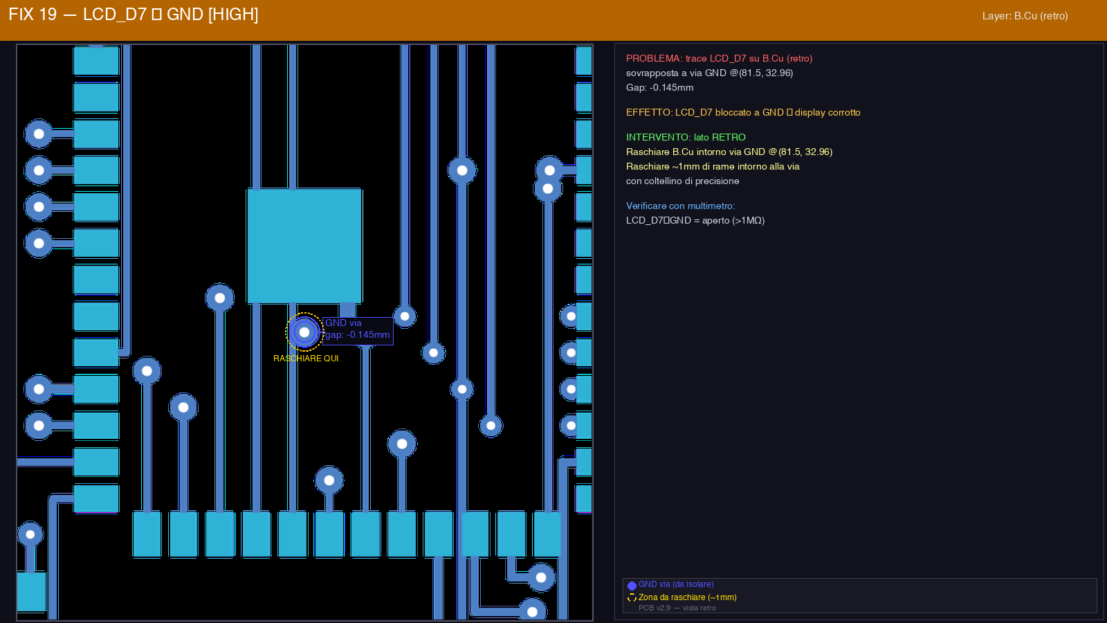
FIX 19 — LCD_D7 → GND (B.Cu)
| Trace | Via | Gap | Effect | Fix |
|---|---|---|---|---|
| LCD_D7 | GND @ (81.5, 32.96) | -0.145mm | Corrupted display | Scrape the B.Cu around the via |
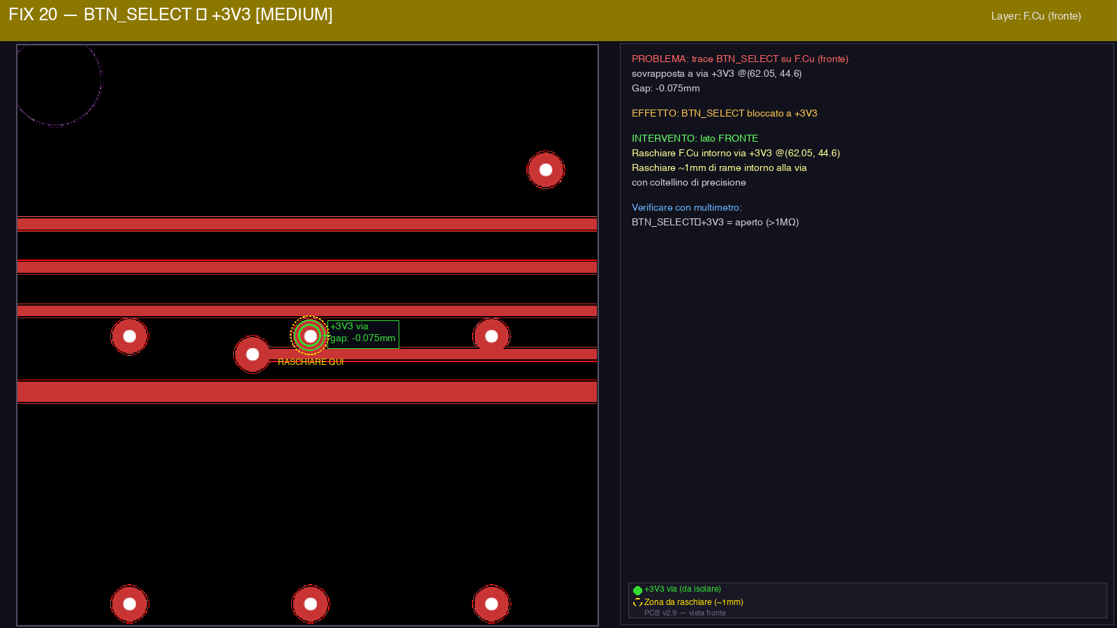
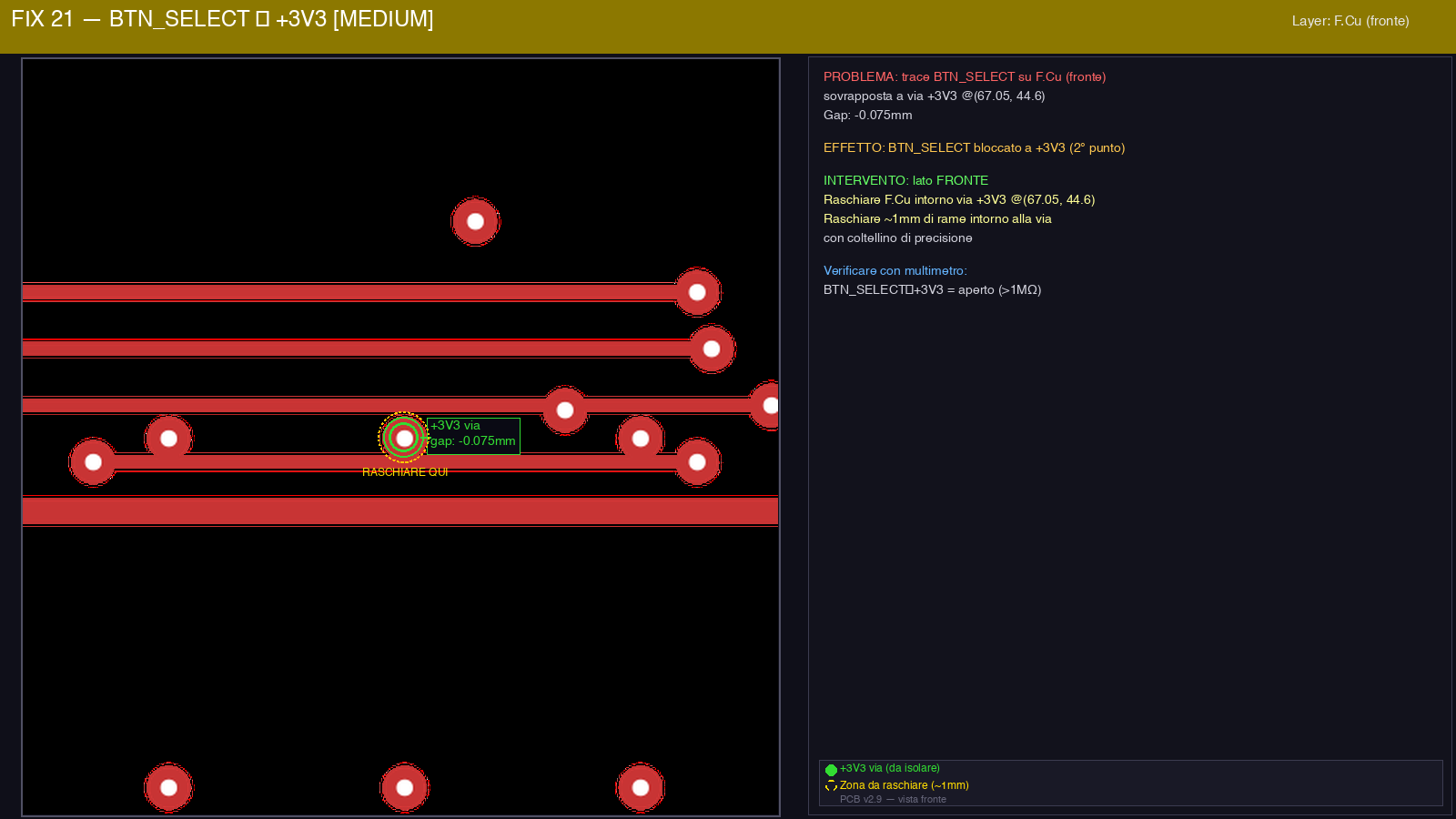
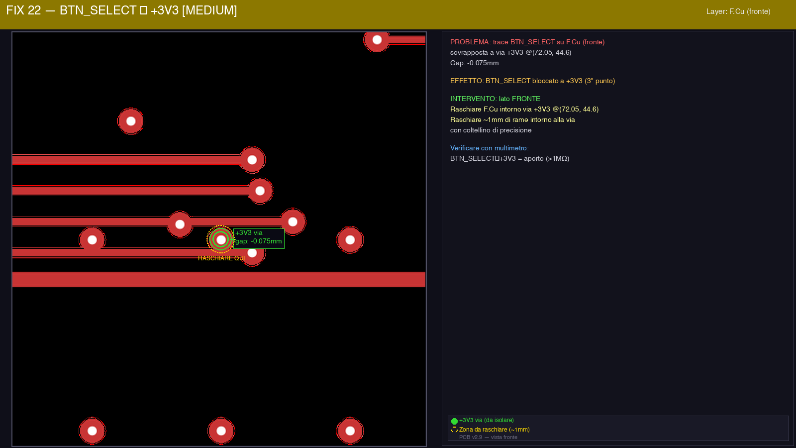
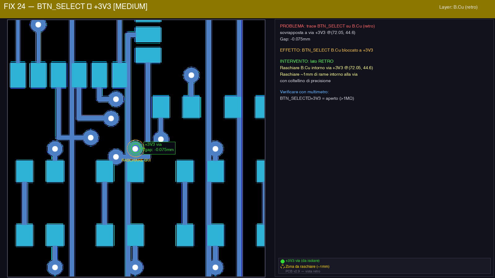
FIX 20-22, 24 — BTN_SELECT → +3V3 (F.Cu + B.Cu, 4 spots)
| # | Layer | Via | Gap |
|---|---|---|---|
| 20 | F.Cu | +3V3 @ (62.05, 44.6) | -0.075mm |
| 21 | F.Cu | +3V3 @ (67.05, 44.6) | -0.075mm |
| 22 | F.Cu | +3V3 @ (72.05, 44.6) | -0.075mm |
| 24 | B.Cu | +3V3 @ (72.05, 44.6) | -0.075mm |
Note: gap -0.075mm — this may not manifest on every fabricated board.
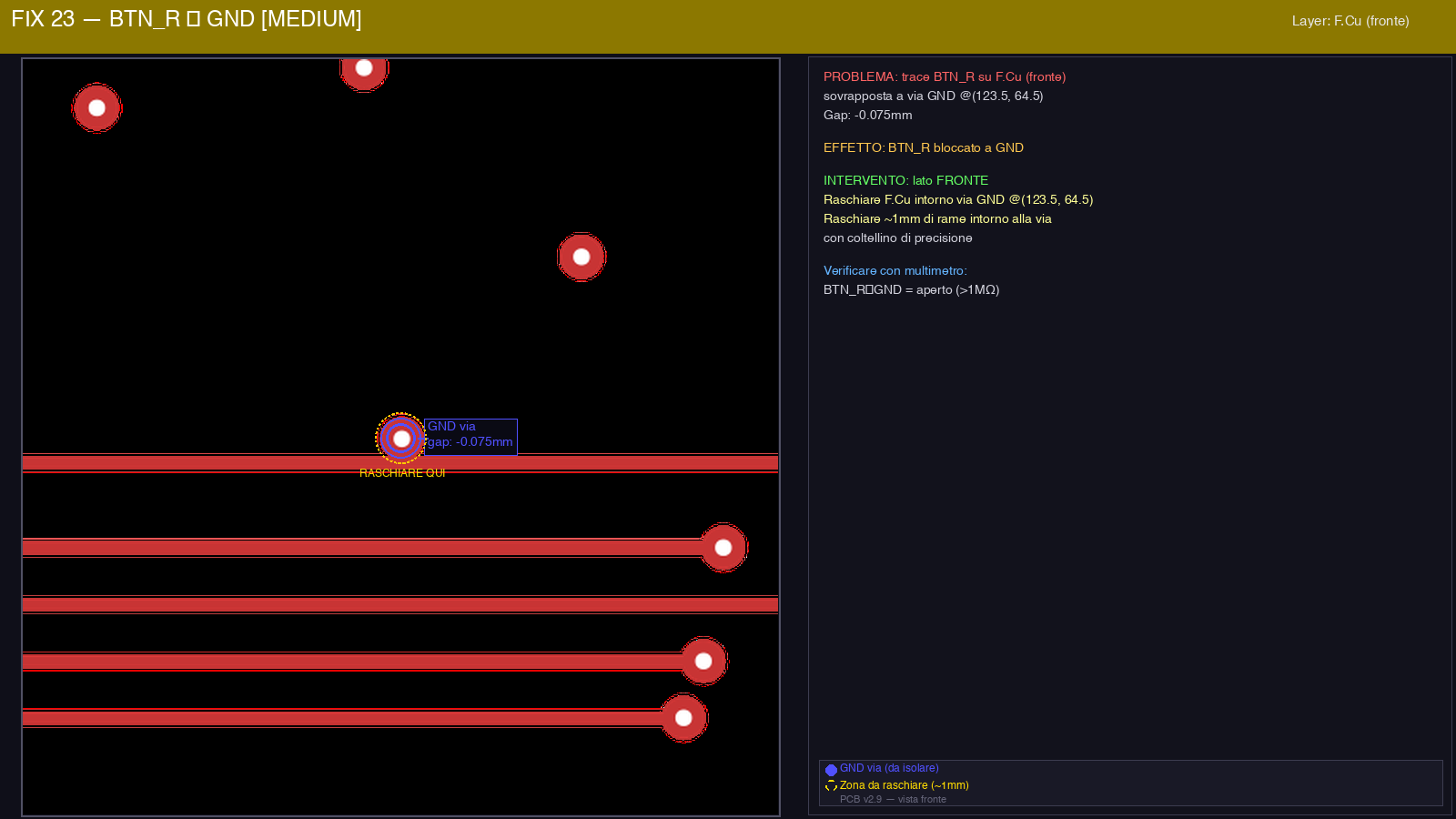
FIX 23 — BTN_R → GND (F.Cu)
| Trace | Via | Gap | Effect | Fix |
|---|---|---|---|---|
| BTN_R | GND @ (123.5, 64.5) | -0.075mm | BTN_R stuck LOW | Scrape the F.Cu around the via |
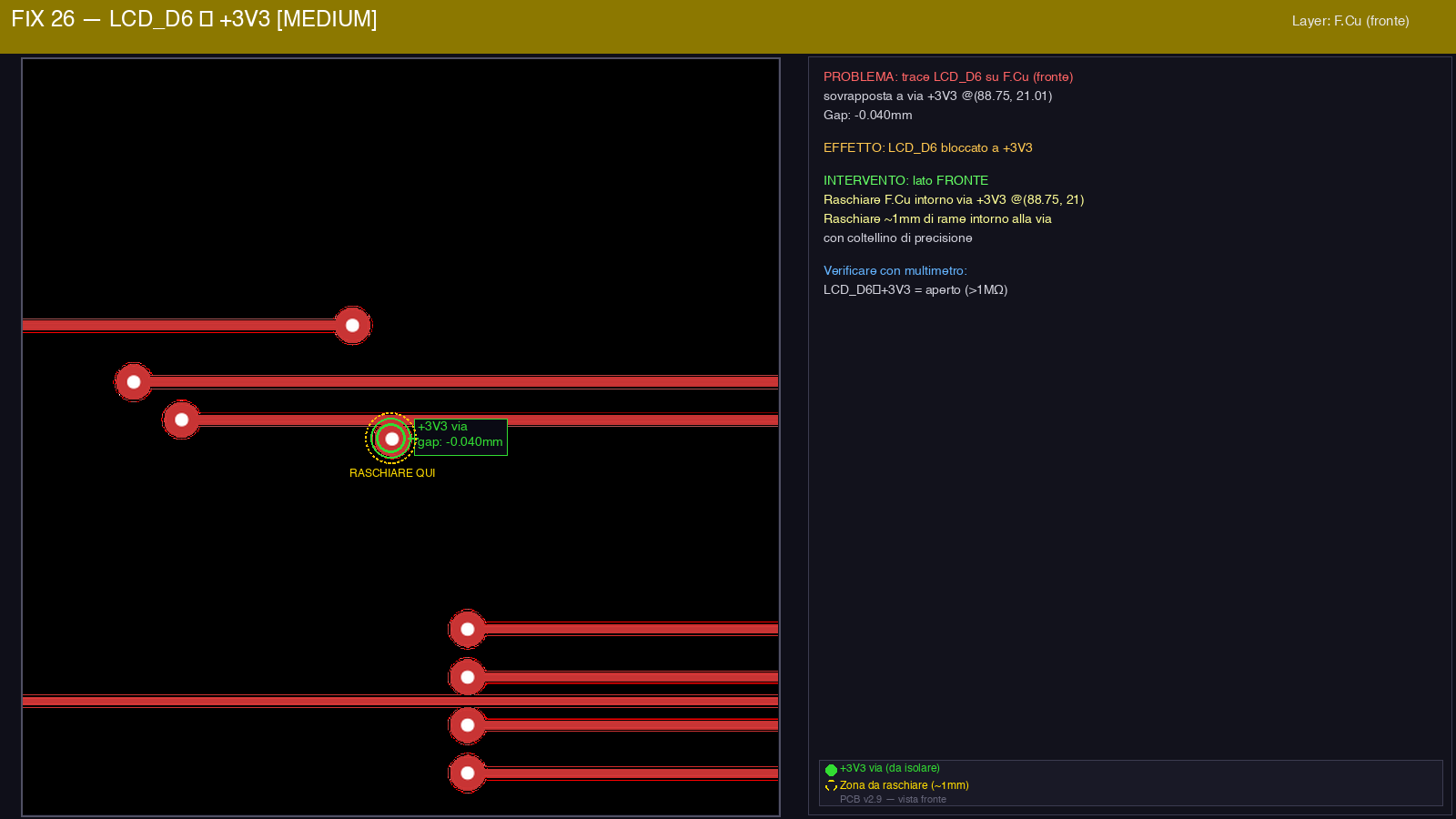
FIX 26 — LCD_D6 → +3V3 (F.Cu)
| Trace | Via | Gap | Effect | Fix |
|---|---|---|---|---|
| LCD_D6 | +3V3 @ (88.75, 21.01) | -0.040mm | Corrupted display | Scrape the F.Cu around the via |
FIX 27 — LCD_D4 → VBUS (B.Cu)
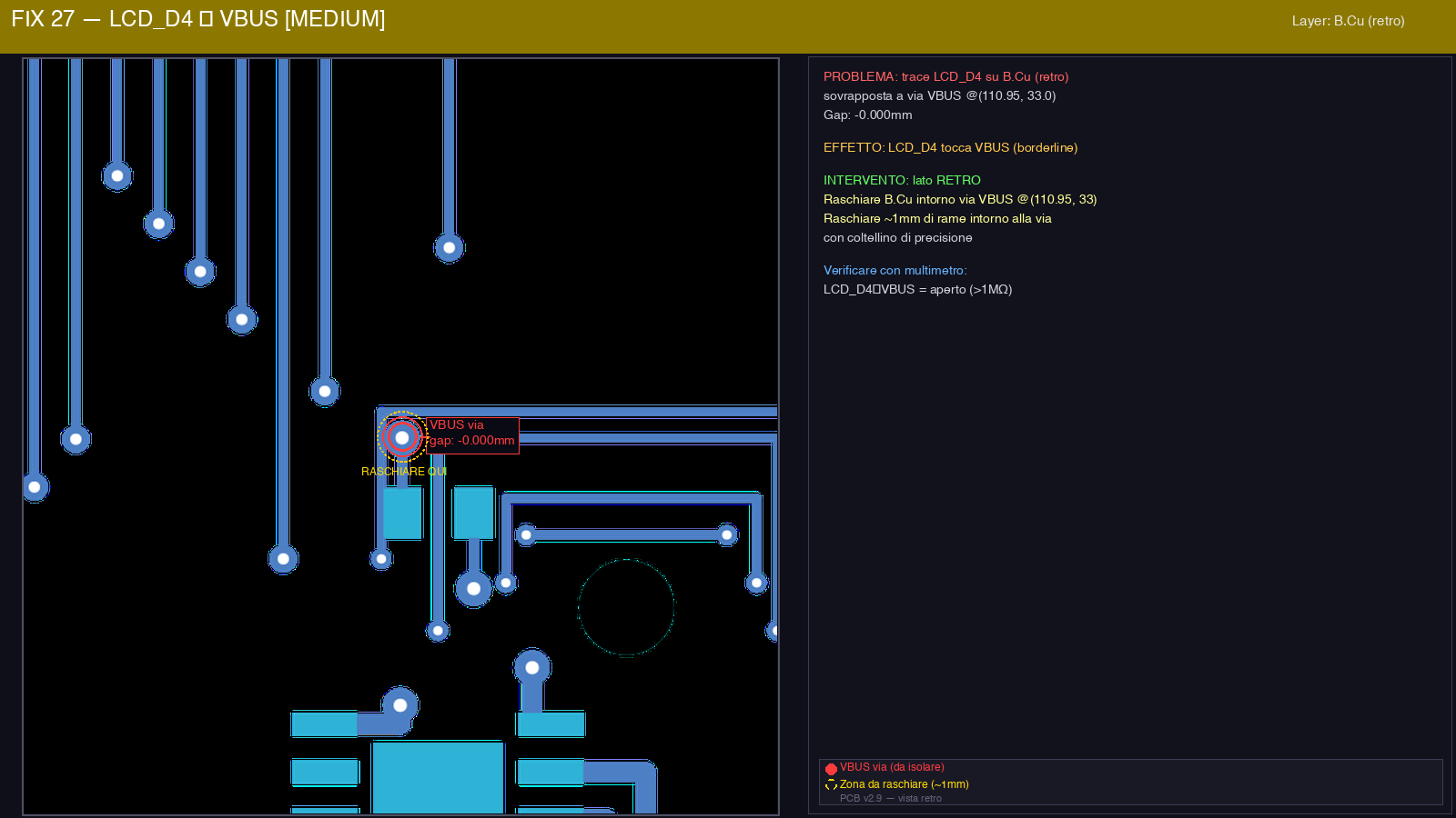
| Trace | Via | Gap | Effect | Fix |
|---|---|---|---|---|
| LCD_D4 | VBUS @ (110.95, 33.0) | -0.000mm | LCD_D4 borderline | Scrape the B.Cu around the via (preventive) |
Post-Rework Checklist
After all the fixes, verify with a multimeter in continuity mode:
| Test | Pad 1 | Pad 2 | Expected | After FIX |
|---|---|---|---|---|
| VBUS-GND | C17+ | C17- | >1MΩ | FIX 1, 3 |
| +5V-GND | C1+ | C1- | >1MΩ | FIX 2, 3 |
| +3V3-GND | C2+ | C2- | >1MΩ | FIX 4-8 |
| BAT+-GND | C18+ | C18- | >1MΩ | FIX 3 |
The +3V3 bulk capacitor on this board was C2, the 22 µF tantalum on the AMS1117 output. Both parts are gone from the current design — the SY8089 buck's ceramic C30 replaced C2. On a current board, probe C30 instead.
Assessment
This v2.9 board carries 44 routing violations, of which 27 are real short circuits. The current PCB (post-v2.9) resolved all of them in the Python generator — DFM was 114/114 pass with 0 collisions at the time, and the suite has since grown to 124 tests.
For v2.9 boards already fabricated, fixes 1-3 are essential. Fixes 4-8 restore the power rails. Fixes 9-27 are required for full functionality (display, buttons, SD card).