First boot — a linear, staged session
One page, one path, no branching unless a light stays dark. Designed for bench-instrument-free commissioning: the diagnostic LEDs and a multimeter on the gated test points are the only instruments, and the battery is connected last, only after the circuit has proven itself on USB power alone.
Connecting the battery is always a LIVE operation on this board: SW16 is not in series with the cell (permanent invariant, respin included — the switch cannot cut battery power). Therefore:
- battery is the LAST thing connected, never the first;
- never connect a battery to a board with a suspected short (the C2-reversed incident was a 0 Ω short on +3V3 — on USB it is current-limited by F1 2A; on a 5000 mAh LiPo it is a fire risk);
- when connecting or disconnecting the battery, unplug USB first.
This does not change on a respin board. The respin/sw16-5v-switch
fix puts Q2 on the +5V load rail, not on the cell: J3 → Q1 → BAT+ →
IP5306 pin 6 is still continuous copper in both switch positions, by
design, because that is what keeps charging alive with the switch OFF.
So "SW16 OFF" is never a substitute for unplugging J3, and connecting
the battery is still a live operation.
This page is written for a board where the switch does nothing. On a
board built from respin/sw16-5v-switch the switch is real, and it gates
the +5V loads through the high-side P-MOSFET Q2:
- SW16 OFF — every load is dead (5V LED, 3V3 LED, HB LED all dark), but USB still charges the cell: the charge path is upstream of Q2. A charging board with a dark LED bank is the expected OFF state, not a fault.
- SW16 ON — the loads come up. There is a deliberate ~1.5 ms soft-start ramp (C32 on Q2's gate) that holds inrush to ~167 mA instead of amps, but it is far too fast to see: to the eye the rail is instant.
- On battery, flipping to ON also has to wake the IP5306. Its boost latches off after 32 s under 45 mA, which the OFF state always triggers, so C33 injects a KEY pulse on the ON transition. If a respin board will not start from the cell after being switched off — but does start the moment you plug USB in — that is the C33 wake pulse being too short, and it is the one BENCH-VALIDATE value in the design. There confirmation is SW17, the do-not-place momentary sitting next to C33 on the KEY node: solder one on and press it. If the board starts on the button but not on the switch, the diagnosis is confirmed and the fix is a larger C33. (SW17 is C720477; it is in the BOM marked DO NOT PLACE, so it ships unpopulated and the land is there waiting.)
Keep SW16 ON for the whole session below. Every stage from 1 onward assumes the loads are powered.
What you need
USB-C cable + any USB PSU (a PC port is fine and current-limits harder), a multimeter, a phone camera. Not yet: battery, SD card, closed case. Keep the case open — the LEDs and test points are read bare.
Where the LEDs are
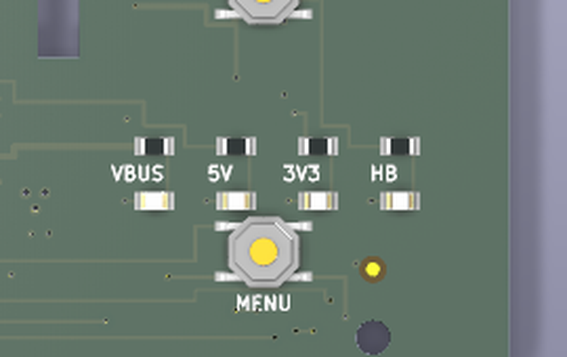
All four diagnostic LEDs sit in one silk-labelled bank on the top side, right edge, just above the MENU button — one glance (or one photo) reads the whole power tree, left to right in the same order the stages below walk it: VBUS → 5V → 3V3 → HB.
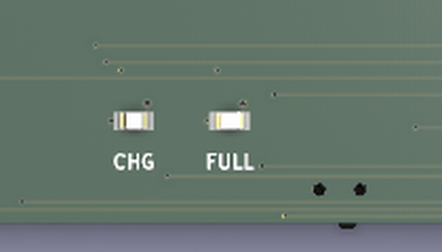
The IP5306 charge-status pair (CHG / FULL) sits near the bottom-left corner and only joins the session at Stage 4, battery in:
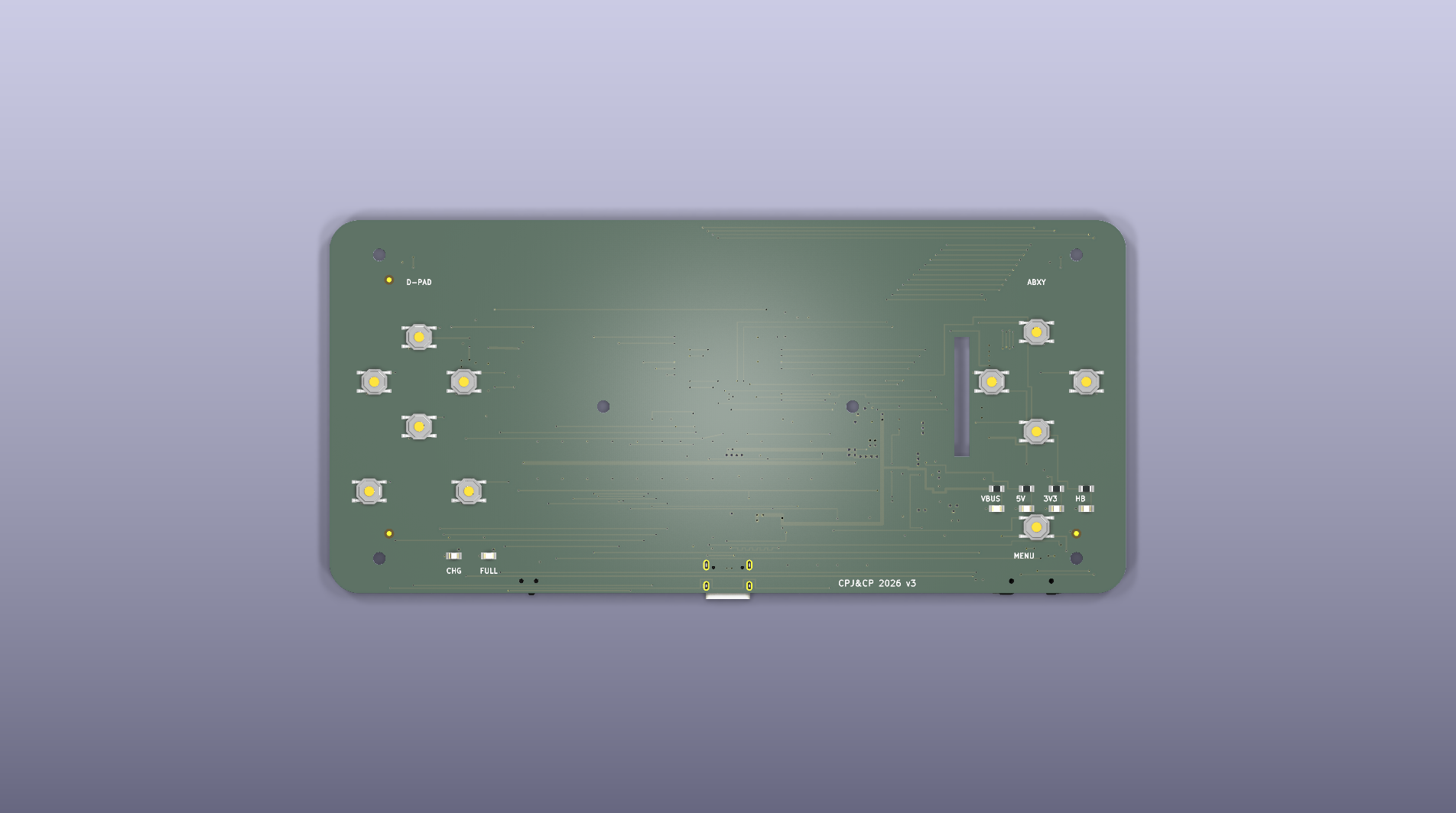
Full board for orientation — the bank is on the right edge, the charge pair on the lower left:
The session log
Copy this table; fill one row per stage. A stage is done only when its exit criterion is met and photographed.
| Stage | Exit criterion | Photo | Notes |
|---|---|---|---|
| 0 pre-flight | board matches renders, both sides | ☐ | |
| 1 USB only | VBUS LED on | ☐ | |
| 2 rails | 5V/3V3 LEDs noted + TP voltages | ☐ | |
| 3 boot | HB LED 1 Hz + BRINGUP verdict | ☐ | |
| 4 battery | boots from cell alone, charge LEDs sane | ☐ | |
| 5 subsystems | blink codes clear one by one | ☐ |
Stage 0 — visual pre-flight (no power at all)
Compare both board sides against the raytraced renders
(release_jlcpcb/renders/), per package family — the v4.3.1 order was
lost to rotations that one photo comparison would have caught. Check the
tantalum stripe, diode cathodes, IC pin-1 dots against
hardware/datasheets/POLARITY_AUDIT.md. With the multimeter in
continuity mode: GND↔+3V3, GND↔+5V, GND↔VBUS must NOT beep
(test points: GND on the U1 module pad, +3V3 on the L2 pad, +5V on the
R27 pad, VBUS on the F1 pad). A beep here ends the session before it
starts — see rework/incident-c2-reversed.
Stage 1 — USB only, nothing else
Plug USB-C. Look at one LED only:
- VBUS lit → cable, connector and fuse F1 are good. Stage done.
- VBUS dark → no board power: try the other cable orientation, another cable, then check F1 continuity and the USB-C solder. Nothing else on the board is meaningful while VBUS is dark.
Respin note: the VBUS LED sits upstream of Q2, so it is lit on USB in both switch positions — that is the point of the design, and it is also the cheapest switch test on the board. Set SW16 OFF: VBUS stays lit (USB is still charging) while the 5V and 3V3 LEDs go dark. Set it back to ON before Stage 2.
Stage 2 — rails, by observation
Still USB only. Read the next two LEDs left to right:
- 5V LED: the IP5306's behavior without a battery is not
established by its datasheet (the model records it as such) — so both
outcomes are informative, neither is a failure yet:
- lit → the power path feeds the rail even batteryless; continue.
- dark → expected-possible without a cell. Confirm with the multimeter on the R27 test point. If you want the digital stages now without a battery, feed 5 V from a sacrificed USB cable directly to the +5V test point (F1 stays upstream); otherwise the 5V/3V3/HB checks simply move after Stage 4.
- 3V3 LED (only meaningful once 5V is present): lit → buck alive. Cross-check with the multimeter: BUCK_FB test point = 0.600 V and +3V3 (L2 pad) ≈ 3.33 V. 3V3 dark with 5V lit → buck stage: U3 orientation, R25/R26 divider, or a rail short — the incident docs for the split plane and C2 are the map.
Stage 3 — boot and heartbeat
With 3V3 present, the HB LED answers the only question that matters: did the chip boot?
- 1 Hz steady blink → boots, straps fine, firmware running.
- dark → power is fine but boot is not: probe EN (test point; must rise to 3.3 V — R3/C31 delay it ~ms, not visibly), then BTN_SELECT (the GPIO0 strap — must read high; a stuck SW14 holds it low and the chip is in download mode).
- repeating N-blink code or fast flutter → it boots AND it is telling you which subsystem failed — jump to Stage 5's table.
Then connect the same USB to a PC and open the serial port: the
bring-up firmware prints its 58-check report
(protocol); BRINGUP-SUMMARY and
BRINGUP-LED must agree with what the LED shows. The bring-up firmware
assumes the board is already powered — it has no model of the power
switch and never mentions it — so on a respin board it requires SW16 ON;
with the switch OFF there is no +3V3, the chip never boots, and there is
no serial port to open.
Stage 4 — battery, at last
Only now, and only if Stage 3 ended green (or Stage 2 ended in the "needs a cell" branch):
- Unplug USB.
- Connect the 105080 cell to J3 — remember: live connection, correct polarity is on you (J3 is keyed; still check red-to-BAT+ against the silk before pushing).
- The board must now boot from the cell alone: 5V → 3V3 → HB 1 Hz with no USB attached. This proves the boost path (U2, L1, the BAT+ copper).
- Re-plug USB with the battery in: LED1/LED2 (the IP5306 charge status pair) join in; charging plus running is the charge-and-play path. Warm is normal, hot is not.
Respin boards — the switch earns its two extra checks here, and this is the only stage where they can be made, because both need a cell:
- USB in, SW16 OFF → charge-only. VBUS LED lit, CHG lit, and the 5V
/ 3V3 / HB LEDs all dark. The cell charges with the system powered
down. If 3V3 survives the switch going OFF, Q2 is not switching —
suspect its orientation (SOT-23-3, source on
+5V_VOUT) or a solder bridge across it, and stop before assuming the rest of the board. - USB out, SW16 OFF for a full minute, then ON → the wake test. One
minute guarantees the IP5306's 32 s light-load shutdown has fired, so
this exercises the C33 KEY pulse and nothing else. The board must come
back up on the cell alone. If it does not, but comes straight up when
USB is plugged in, the wake pulse is short. Log it and take the
measurement: scope
IP5306_KEYagainst GND across the ON transition and record the pulse width and depth. C33 is the design's one BENCH-VALIDATE value and this is the measurement that closes it — its RC runs against the IP5306's undocumented internal KEY pull-up, so the number cannot be derived, only measured. To separate a short pulse from a dead wake path, fit SW17 (the do-not-place momentary beside C33) and press it: if that wakes the board, the path is fine and only the pulse is short.
Never use the switch to "disconnect the battery" for a rework: it does not, by design. Unplug J3.
Stage 5 — subsystems, one insertion at a time
Insert/connect one thing, power-cycle (unplug both, battery too, if the step involves a connector), re-run, read the code:
| Blink code | Subsystem | First things to probe when it persists |
|---|---|---|
| 2 | SD | card seated, SD_CS/CLK/MISO/MOSI test points (all on U1 pads) |
| 3 | Display | J4 FPC seated straight (41−N pin reversal is by design — do NOT "fix" cabling), LCD_WR/DC/CS TPs |
| 4 | Audio | speaker wiring, PAM8403 |
| 5 | Buttons | the named button's net vs GND when pressed |
| 6 | PSRAM | module solder (reflow-class problem — stop and document) |
| fast flutter | none of the above | read the serial report — the failure has no LED code |
The session ends when BRINGUP-SUMMARY says verdict=GREEN on
battery power with the case still open. Only then close the case.
If a stage will not pass
Do not improvise reworks mid-session. Photograph, note the stage and
the exact LED/TP readings in the session log, and open the matching
incident doc under rework/ — every dark-LED pattern above maps to a
documented failure class. A new failure class earns a new incident doc
before it earns a soldering iron.