Bill of Materials (BOM) with AliExpress Links
All components selected for the prototype, with direct purchase links.
Interactive BOM viewer: Open Interactive BOM — click any component to highlight it on the PCB layout (dark mode, pin-1 markers).
MCU — ESP32-S3
| Option | Flash | PSRAM | USB | Price | Link |
|---|---|---|---|---|---|
| ESP32-S3 DevKitC-1 N16R8 (clone) | 16 MB | 8 MB Octal | Dual USB-C | $5.50-$7.00 | AliExpress |
| WeAct ESP32-S3-A N16R8 | 16 MB | 8 MB Octal | Dual USB-C | $5.50-$7.50 | AliExpress (WeAct Store) |
| Waveshare ESP32-S3-DEV-KIT N16R8 | 16 MB | 8 MB Octal | USB-C | $10.99-$12.99 | Waveshare |
Recommended: ESP32-S3 DevKitC-1 N16R8 generic (~$6.00)
Display
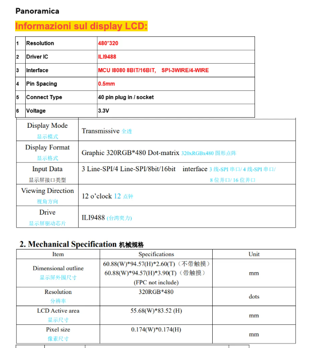
Chosen: ILI9488 3.95" Bare LCD Panel (for custom PCB)
| Spec | Value |
|---|---|
| Size | 3.95" |
| Resolution | 320(RGB) × 480 |
| Controller | ILI9488 |
| Touch | Resistive (SPI) — not connected, touch not used |
| Connector | 40-pin FPC, 0.5mm pitch |
| Interface | MCU 8/16-bit parallel + SPI |
| Backlight | White LED, 3.3V |
| Display colors | 262K |
| Price | ~$3.95 |
| Link | AliExpress |
The bare LCD panel connects directly to the PCB via a 40-pin FPC ribbon — no breakout PCB, no pin headers. This is how commercial handheld consoles are built: compact, thin, and plug-in. The FPC ribbon slides into the J4 connector on our PCB and locks with the latch. Zero soldering required.
Both controllers are equivalent for 8-bit 8080 parallel with RGB565 (~20 MB/s). Key differences:
- ESP-IDF: use community component
esp_lcd_ili9488(ST7796S has official Espressif component) - LovyanGFX / TFT_eSPI: both controllers fully supported
- SPI limitation: ILI9488 does NOT support RGB565 over SPI (only RGB666/888). This does not affect us since we use parallel 8080.
- Init sequence: slightly different command set, but handled by the driver library
Display Orientation (landscape for gaming)
Portrait (native)          Landscape (gaming mode)
┌──────────┐               ┌─────────────────────┐
│          │               │                     │
│  320px   │    rotate     │      480px          │
│    ×     │   -------->   │       ×             │
│  480px   │    90° CW     │      320px          │
│          │               │                     │
│  FPC ══  │               │              FPC ══ │
└──────────┘               └─────────────────────┘
FPC 40-Pin Pinout (ILI9488 panel datasheet)
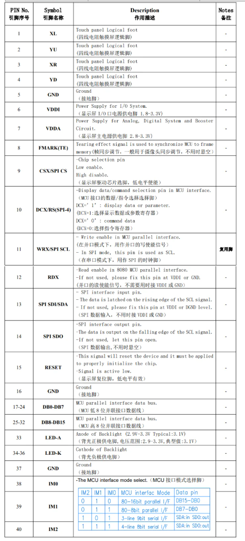
| Pin | Symbol | Direction | Description | Connection |
|---|---|---|---|---|
| 1 | XL | — | Touch panel logical foot | NC |
| 2 | YU | — | Touch panel logical foot | NC |
| 3 | XR | — | Touch panel logical foot | NC |
| 4 | YD | — | Touch panel logical foot | NC |
| 5 | GND | — | Ground | GND |
| 6 | VDDI | — | I/O power supply (1.8–3.3V) | +3V3 |
| 7 | VDDA | — | Analog/digital power (2.8–3.3V) | +3V3 |
| 8 | TE | Output | Tearing effect (vsync) | NC |
| 9 | CS | Input | Chip select (active low) | GPIO12 |
| 10 | DC/RS | Input | Data/Command select | GPIO14 |
| 11 | WR | Input | Write strobe (8080 mode) | GPIO46 |
| 12 | RD | Input | Read strobe (8080 mode) | +3V3 (tied HIGH) |
| 13 | SPI SDI | Input | SPI data in | NC (parallel mode) |
| 14 | SPI SDO | Output | SPI data out | NC (parallel mode) |
| 15 | RESET | Input | Reset (active low) | GPIO13 |
| 16 | GND | — | Ground | GND |
| 17-24 | DB0-DB7 | I/O | 8-bit parallel data bus | GPIO4-11 |
| 25-32 | DB8-DB15 | I/O | 16-bit extension | NC (8-bit mode) |
| 33 | LED-A | — | Backlight anode (2.9–3.3V typ 3.1V) | +5V via R27 20Ω (net LED_BLA, always-on, ~90 mA defined by the family class rating — R25-HIGH-1 fixed in the design 2026-07-31; every board fabricated through v4.3.1 carries the old hard +3V3 tie with no current-limiting element) |
| 34-36 | LED-K | — | Backlight cathode (8 chip white LED) | GND |
| 37 | GND | — | Ground | GND |
| 38 | IM0 | Input | Interface mode select | +3V3 (HIGH) |
| 39 | IM1 | Input | Interface mode select | +3V3 (HIGH) |
| 40 | IM2 | Input | Interface mode select | GND (LOW) |
| IM2 | IM1 | IM0 | Mode | Data Pins |
|---|---|---|---|---|
| 0 | 1 | 0 | 8080 16-bit parallel | DB15-DB0 |
| 0 | 1 | 1 | 8080 8-bit parallel | DB7-DB0 |
| 1 | 0 | 1 | 3-line 9-bit SPI | SDA in/out |
| 1 | 1 | 1 | 4-line 8-bit SPI | SDA in/out |
Our design uses 8080 8-bit parallel (IM2=0, IM1=1, IM0=1): IM0 and IM1 pulled HIGH to +3V3, IM2 pulled LOW to GND.
This pinout is from the actual ILI9488 3.95" panel datasheet (see images above). It differs significantly from generic/typical pinouts found online. Do NOT use generic ILI9488 pinout tables — always refer to this datasheet.
When the display is mounted in landscape (CCW rotation), Pin 1 is at the south end of the FPC tail. The ribbon passes straight through the PCB slot to J4 on the bottom side without twisting, so display Pin N contacts connector Pad (41−N). The PCB traces are routed accordingly — e.g., display Pin 17 (DB0/GPIO4) connects to J4 Pad 24. See PCB FPC Slot for details.
Alternative Display Options
| Option | Size | Resolution | Controller | Interface | Price | Notes |
|---|---|---|---|---|---|---|
| ST7796 4.0" bare panel + GT911 touch | 4.0" | 320x480 | ST7796S | 8/16-bit parallel | ~$8-12 | AliExpress — larger screen, official ESP-IDF driver |
| ST7796S 4.0" module + PCB | 4.0" | 320x480 | ST7796S | 8/16-bit parallel | ~$12-19 | Prototyping only (pin headers, no FPC) |
| ST7796S 3.5" IPS SPI | 3.5" | 320x480 | ST7796S | SPI | $8-$12 | Prototyping only |
Power Supply
LiPo Battery
| Option | Capacity | Dimensions | Weight | Price | Link |
|---|---|---|---|---|---|
| LiPo 105080 5000mAh | 5000mAh | 50x80x10mm | ~80g | ~$5-8 | AliExpress |
| LiPo 104060 3000mAh | 3000mAh | 40x60x10mm | ~50g | $6.70 | AliExpress |
| LiPo 103450 2000mAh | 2000mAh | 34x50x10mm | ~35g | $3.50 | AliExpress |
USB-C Charging Module
| Option | Features | Price | Link |
|---|---|---|---|
| IP5306 USB-C | Charge+boost 5V/2.4A, charge-and-play | $1.59 | AliExpress |
| TP4056 USB-C | Charge only 1A, no boost (needs external regulator) | $0.25 | AliExpress |
Voltage Regulator
| Option | Specification | Price | Link |
|---|---|---|---|
| SY8089AAAC | 2A synchronous buck 5V->3.3V, ~93% | $0.12 | LCSC C78988 |
Recommended: LiPo 5000mAh + IP5306 + SY8089AAAC buck (~$7-10)
About 12.9 hours of continuous gameplay. That is not 5000 / load — the number
is derived through both conversion stages (SY8089 buck at ~93 %, IP5306 boost at
~90 %) in Power Budget, which is the single place it
is computed.
USB-C -> [IP5306] -> +5V_VOUT -> [Q2 PMOS] -> +5V -> [SY8089 buck] -> 3.3V -> ESP32-S3
            |                        ^
       [LiPo Battery]           SW16 (gate)
The IP5306 manages battery charge/discharge and provides a stable 5V output on
+5V_VOUT. Since the SW16 respin, the high-side P-MOSFET Q2 separates that
boost output from the +5V load rail: SW16 only drives Q2's gate, so OFF kills
every load while USB charging (upstream of Q2) keeps working. The SY8089AAAC synchronous buck steps it down to 3.3V at ~93% efficiency. A linear regulator was used up to v1: at 5V in / 3.3V out it can only ever be 66% efficient, dissipating ~0.46W typical and ~1.0W at peak inside a sealed enclosure. The buck dissipates ~0.07W for the same load.
Controls / Input
| Component | Specification | Price | Link |
|---|---|---|---|
| Tact switch 6x6mm (20pcs) | Momentary push button, for D-pad/A/B/X/Y/Start/Select/L/R (12 buttons) | $1.04 | AliExpress |
| Rubber pads GBA-style | Conductive silicone, better feel | $0.27 | AliExpress |
| Rubber pads GBA full set | D-pad + A/B + Start/Select + L/R | $1.05 | AliExpress |
| Removed in v2 — GPIOs reassigned to USB data and BTN_R |
Audio
| Component | Specification | Price | Link |
|---|---|---|---|
| Speaker 28mm 8ohm 0.5W | Mini speaker (5pc pack $4.05) | $0.81/pc | AliExpress |
| PAM8403 amplifier | 2ch 3W, with volume pot | $0.44 | AliExpress |
Storage
| Component | Specification | Price | Link |
|---|---|---|---|
| SD Card module SPI | Micro SD reader, built-in level shifter | $0.45 | AliExpress |
| Micro SD 32GB | Class 10 / UHS-I (Kingston or Samsung) | $3.50 | AliExpress |
Prototyping Supplies
| Component | Specification | Price | Link |
|---|---|---|---|
| Breadboard 830 points | For phase 2 prototype | ~$2.00 | AliExpress |
| Jumper wires set | M-M, M-F, F-F | ~$2.00 | AliExpress |
| Resistor/capacitor kit | Assorted values | ~$2.00 | AliExpress |
Budget Summary
Recommended Configuration (SNES Primary)
| Category | Component | Price |
|---|---|---|
| MCU | ESP32-S3 N16R8 DevKitC-1 | $6.00 |
| Display | ILI9488 3.95" 8-bit parallel (bare panel) | $3.95 |
| Battery | LiPo 105080 5000mAh | $6.50 |
| Charging | IP5306 USB-C | $1.59 |
| Regulator | SY8089AAAC buck | $0.12 |
| Controls | Tact switch 20pcs (12 buttons: D-pad, A, B, X, Y, Start, Select, L, R) | $1.04 |
| Extra controls | Rubber pads | $1.05 |
| Audio | Speaker + PAM8403 | $1.25 |
| Storage | SD module + 32GB card | $3.95 |
| Misc | Breadboard, jumpers, resistors | $6.00 |
| TOTAL | $32.90 |
Button Layout
    [L]                         [R]

                            [X]
  [D-pad]              [Y]     [A]
  up/down/                  [B]
  left/right

        [Select] [Start]
12 buttons total: D-pad (4), A, B, X, Y, Start, Select, L, R
Plan for ~$45 to have margin for spares and unexpected needs — the project's stated prototype budget band is $33–45.
Most AliExpress sellers offer free shipping. Delivery time: 2-4 weeks (standard).
JLCPCB PCB Assembly — LCSC Part Numbers
For the custom PCB version (see PCB Design), all SMT components are sourced from LCSC for JLCPCB assembly.
38 line items, 99 placements. Generated from release_jlcpcb/bom.csv — the file uploaded to JLCPCB. Regenerate with make docs-bom.
| Ref | Part | Package | LCSC | Qty | Role | Datasheet |
|---|---|---|---|---|---|---|
| U1 | ESP32-S3-WROOM-1-N16R8 | Module_ESP32-S3-WROOM-1 | C2913202 | 1 | ESP32-S3-WROOM-1-N16R8 — 16 MB flash, 8 MB octal PSRAM | |
| U2 | IP5306 | ESOP-8 | C181692 | 1 | IP5306 — charger + 5 V boost, charge-and-play | |
| U3 | SY8089AAAC 2A Buck | SOT-23-5 | C78988 | 1 | SY8089AAAC — 2 A synchronous buck, 5 V → 3.3 V (~93 %) | |
| U5 | PAM8403 | SOP-16 | C5122557 | 1 | PAM8403 — class-D audio amplifier | |
| J1 | USB-C 16-pin | USB-C-SMD-16P | C2765186 | 1 | USB-C receptacle, 16-pin | |
| U6 | Micro SD Card Slot | TF-01A | C91145 | 1 | microSD slot (TF-01A) — ROM storage | |
| J3 | JST PH 2-pin SMD | JST-PH-2P-SMD | C295747 | 1 | JST PH battery connector | — |
| LED1 | Red LED 0805 | LED_0805 | C84256 | 1 | red LED (LED1) — power indicator on +3V3 (U2's LED pins are NC) | |
| LED2 | Red LED 0805 | LED_0805 | C19171391 | 1 | red LED — LED2 power indicator / LED3-6 diagnostics; YLED0805R is red despite the old 'green' label | |
| L1 | 1uH 4.5A Inductor | SMD-4x4x2mm | C280579 | 1 | L1 — IP5306 boost inductor | |
| L2 | 2.2uH 2.95A Inductor | IND-SMD-4.0x4.0 | C36409 | 1 | L2 — SY8089 buck output inductor | — |
| R1,R2 | 5.1k 0805 | R_0805 | C27834 | 2 | CC1/CC2 pull-downs — USB-C UFP detection | |
| R3,R4,R5,R6,R7,R8,R9,R10,R11,R12,R13,R15 | 10k 0805 | R_0805 | C17414 | 12 | button pull-ups + R3 EN pull-up (R25-CRIT-1 fix) | |
| R20,R21 | 20k 0805 | R_0805 | C4328 | 2 | PAM8403 INL/INR input bias | — |
| R24,R25 | 100k 0805 | R_0805 | C149504 | 2 | R24 Q1 gate pull-down, R25 buck feedback (upper) — R16 deleted in the SW16 respin | |
| R26,R32 | 22k 0805 | R_0805 | C17560 | 2 | R26 buck feedback (lower), R32 Q2 gate pull-up (default OFF) | — |
| C29 | 22pF 0805 C0G | C_0805 | C1804 | 1 | C29 — buck feedback feedforward | — |
| R17,R18,R33 | 1k 0805 | R_0805 | C17513 | 3 | R17/R18 LED series resistors + R33 Q2 series gate resistor (soft-start slope) | |
| C3,C4,C5,C6,C7,C8,C9,C10,C11,C12,C13,C14,C15,C16,C21,C26,C31 | 100nF 0805 | C_0805 | C49678 | 17 | decoupling + C31 EN reset cap (R25-CRIT-1 fix) | |
| C22 | 0.47uF 0805 | C_0805 | C13967 | 1 | C22 — DC-blocking into PAM8403 | — |
| C23,C24,C25,C32 | 1uF 0805 | C_0805 | C28323 | 4 | PAM8403 VDD/PVDD decoupling + C32 Q2 gate-source soft-start cap | — |
| C33 | 4.7uF 0805 | C_0805 | C1779 | 1 | C33 — IP5306 KEY wake cap (couples the SW16 ON transition into KEY) | — |
| C17,C18,C27 | 10uF 0805 | C_0805 | C15850 | 3 | bulk decoupling | |
| C1,C19,C30 | 22uF 1206 MLCC | C_1206 | C12891 | 3 | C1 buck input, C19 boost output, C30 buck output | |
| SW1,SW2,SW3,SW4,SW5,SW6,SW7,SW8,SW9,SW10,SW11,SW12,SW13,SW15,SW14 | SMT Tact Switch 5.1x5.1mm | SW-SMD-5.1x5.1 | C318884 | 15 | tact switches — D-pad, ABXY, Start/Select, L/R, Menu, RST, BOOT | |
| J4 | FPC 40-pin 0.5mm Bottom Contact | FPC-40P-0.5mm | C2856812 | 1 | FPC 40-pin 0.5 mm — ILI9488 display | |
| SW16 | Slide Switch SS-12D00G3 | SS-12D00G3 | C431540 | 1 | SW16 slide switch (MSK12C02) — drives Q2's gate; carries no rail current | |
| U4 | USBLC6-2SC6 USB ESD TVS | SOT-23-6 | C7519 | 1 | USBLC6-2SC6 — USB ESD/TVS protection | — |
| R22,R23 | 22R 0402 | R_0402 | C25092 | 2 | USB D+/D- series termination | — |
| R27 | 20R 1206 | R_1206 | C17955 | 1 | R27 — backlight series resistor, +5V -> LED_BLA (R25-HIGH-1 fix) | — |
| F1 | PTC Resettable Fuse 2A 1812 | F_1812 | C960026 | 1 | F1 — VBUS PTC fuse, 2A hold / 4A trip (R3-HIGH-4 fix) | — |
| D1 | BAT54C Dual Schottky Diode | SOT-23 | C37704 | 1 | BAT54C — dual Schottky, menu-combo diode OR | — |
| Q1,Q2 | AO3401A P-Channel MOSFET | SOT-23 | C15127 | 2 | AO3401A — Q1 reverse-battery protection, Q2 +5V high-side load switch (R32: replaced SI2301CDS C10487, whose 2.3 A rating sat below the battery-path current) | — |
| LED3,LED4,LED5,LED6 | Red LED 0805 (bring-up diagnostic, DNP in production) | LED_0805 | C19171391 | 4 | red LED — LED2 power indicator / LED3-6 diagnostics; YLED0805R is red despite the old 'green' label | |
| R28,R29 | 5.1k 0805 (bring-up diagnostic, DNP in production) | R_0805 | C27834 | 2 | CC1/CC2 pull-downs — USB-C UFP detection | |
| R30,R31 | 1k 0805 (bring-up diagnostic, DNP in production) | R_0805 | C17513 | 2 | R17/R18 LED series resistors + R33 Q2 series gate resistor (soft-start slope) | |
| R34 | 1M 0805 | R_0805 | C17514 | 1 | — | |
| SW17 | TS-1088 (SMD momentary switch 3.9x3.0mm; DO NOT PLACE - manual IP5306 KEY wake, fit only if the C33 RC needs it) | SW-SMD-2P-TS1088 | C720477 | 1 | SW17 — manual KEY wake, DO NOT PLACE (fit only if the C33 pulse is short) | — |
PCBA cost (real JLCPCB quote): $197.86 for 5 boards (~$39.57/board) including fabrication, components and assembly. Most of it is one-time setup — see the full quote breakdown.
v2 Additional Components (Audio Coprocessor)
The v2 PCB adds an ESP32-S3-MINI-1-N8 as a dedicated audio coprocessor (see Phase 5 — Software Architecture):
| Ref | Component | Package | LCSC | Class | Unit cost |
|---|---|---|---|---|---|
| U7 | ESP32-S3-MINI-1-N8 | Module (15.4×20.5mm) | C2913206 | Extended | $3.25 |
| C34,C35 | 100nF 0805 (decoupling) | 0805 | C49678 | Basic | $0.01 |
v2 BOM delta: +$3.27 per unit. No external crystal, flash, or extra passives needed — the module integrates everything. (References C26–C33 are already taken on the v1 board — C32/C33 are the SW16 respin's gate and wake caps — so the coprocessor's decoupling caps are C34/C35.)
v2 estimated PCBA cost: $215 for 5 boards ($43/board).
PCB Version — What to Buy Separately
When ordering the custom PCB from JLCPCB, the following components are NOT included in the assembly and must be purchased from AliExpress:
| Component | Ref | Price | Connection to PCB | Solder? |
|---|---|---|---|---|
| ILI9488 3.95" bare LCD panel (40P FPC 0.5mm, resistive touch NC) | — | ~$3.95 | FPC ribbon → J4 connector (slide + latch) | No |
| LiPo 105080 5000mAh battery | BT1 | ~$6-8 | JST PH plug → J3 connector | No |
| Speaker 28mm 8Ω | SPK1 | ~$0.80 | 2 wires → solder pads | Yes (easy) |
| — | Removed in v2 — GPIOs reassigned to USB data and BTN_R | — | ||
| ~$17-23 |
The display and battery are plug-in — no soldering skills required. Only the speaker (2 wires) needs soldering.
Buy the bare LCD panel (no PCB breakout board), specifically:
- ILI9488 controller, 3.95", 320×480, 40-pin FPC 0.5mm pitch
- Resistive touch (not connected — touch pins left NC on PCB)
- AliExpress link
Do NOT buy display modules with PCB breakout + pin headers — those are for breadboard prototyping and won't fit the FPC connector on the PCB.