PCBA Manufacturing & Ordering
Production-ready PCB Assembly (PCBA) ordered from JLCPCB — minimum order of 5 units with full SMT assembly.
All production files in release_jlcpcb/ are verified and ready for ordering:
- 124 DFM tests, 9 DFA assembly tests and 24 JLCPCB validation tests pass
- 48/48 polarity checks, 274 pin-to-net comparisons against the datasheets
- 19 silkscreen labels on F.SilkS/B.SilkS for component identification
- W_PWR_LOW = 0.30mm trace width for power stubs
- 85 placements in BOM/CPL matched against schematic and PCB
- 0 DRC errors, all pre-production checks passed
⚠ Do not fabricate from tag v4.3.1 — that batch died of a systemic CPL
rotation error (incident). Cut a fresh
tag from main, where the rotation law and its gates are in force.
Assembled PCB Preview
Top Side — Controls & LEDs
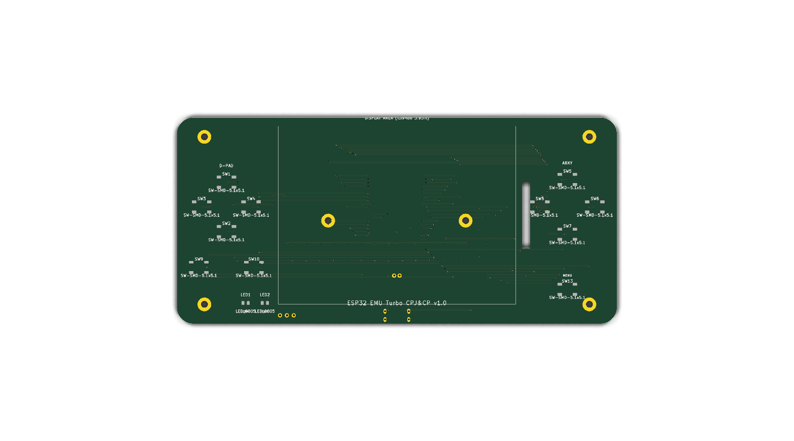
The top side carries all user-facing components:
| Designator | Component | JLCPCB Part # | Footprint |
|---|---|---|---|
| LED1 | Red LED (power indicator) | C84256 | LED_0805 |
| LED2 | Red LED (second power indicator — the "green"/"charged" label was wrong; C19171391 is a red part and U2's LED pins are NC) | C19171391 | LED_0805 |
| SW1–SW10 | SMT tactile buttons (D-pad, ABXY, Start, Select) | C318884 | SW-SMD |
All 12 gaming buttons are surface-mounted on the top face for direct user interaction.
Bottom Side — Core Electronics
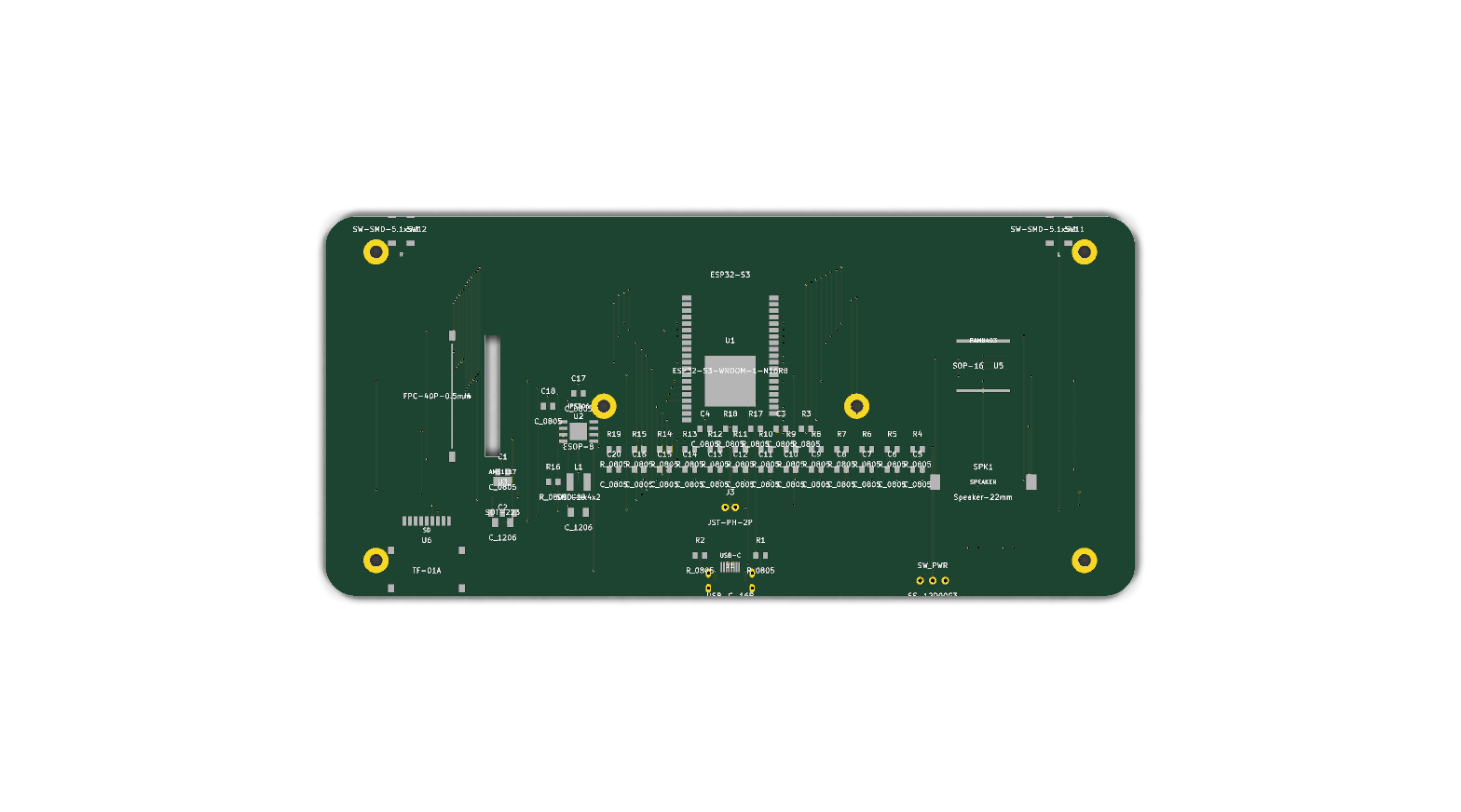
The bottom side hosts the main circuitry:
| Designator | Component | JLCPCB Part # | Footprint |
|---|---|---|---|
| U1 | ESP32-S3-WROOM-1 (N16R8) | C2913202 | Module |
| U2 | IP5306 (charge management) | C181692 | ESOP-8 |
| U3 | SY8089AAAC (2A buck) | C78988 | SOT-23-5 |
| U5 | PAM8403 (audio amplifier) | C5122557 | SOP-16 |
| J1 | USB-C connector (16-pin) | C2765186 | USB-C-SMD |
| J3 | JST-PH 2-pin SMD (battery) | C295747 | JST-PH-2P-SMD |
| J4 | FPC 40-pin 0.5mm (display) | C2856812 | FPC-40P |
| L1 | 1uH 4.5A inductor | C280579 | SMD-4x |
| L2 | 2.2uH 2.95A buck inductor | C36409 | IND-SMD-4.0x4.0 |
| U4 | USBLC6-2SC6 USB ESD TVS | C7519 | SOT-23-6 |
| Q1 / D1 / F1 | RPP MOSFET / BAT54C / 2A PTC fuse | C15127 / C37704 / C960026 | SOT-23 / SOT-23 / 1812 |
| SW16 | Slide switch (power) | C431540 | SS-12D0 |
| SW11, SW12 | SMT tactile (L, R shoulder) | C318884 | SW-SMD |
| R1, R2 | 5.1k (USB-C CC) | C27834 | R_0805 |
| R4–R13,R15 | 10k (pull-ups) | C17414 | R_0805 |
| R17, R18 | 1k | C17513 | R_0805 |
| R20, R21 | 20k (PAM8403 INL/INR bias to VREF) | C4328 | R_0805 |
| C17, C18, C27 | 10uF | C15850 | C_0805 |
| C1, C19, C30 | 22uF (buck in / boost out / buck out) | C12891 | C_1206 |
| C29 | 22pF C0G (buck feed-forward) | C1804 | C_0805 |
| C3–C16,C21,C26,C31 | 100nF | C49678 | C_0805 |
| C22 | 0.47uF (PAM8403 DC-block) | C13967 | C_0805 |
| C23–C25 | 1uF (PAM8403 VDD/PVDD) | C28323 | C_0805 |
| R22,R23 / R24 / R25 / R26 / R27 | 22R USB / 100k gate / 100k FB / 22k FB / 20R backlight | C25092 / C149504 / C149504 / C17560 / C17955 | R_0402 / R_0805 / R_1206 |
| Q2 | AO3401A P-MOSFET — SW16 respin high-side switch, +5V_VOUT → +5V | C15127 | SOT-23 |
| R32 / R33 / R34 | 22k gate pull-up / 1k series gate / 1M PWR_SW→BAT+ | C17560 / C17513 / C17514 | R_0805 |
| C32 | 1uF Q2 gate soft-start | C28323 | C_0805 |
| C33 | 4.7uF IP5306_KEY wake cap (BENCH-VALIDATE) | C1779 | C_0805 |
| SW17 | TS-1088 momentary, IP5306_KEY → GND — DO NOT PLACE (in the BOM so it can be sourced, absent from the CPL) | C720477 | SW-SMD-2P-TS1088 |
Total SMT components: 37 unique part types, 99 BOM placements — 98 of which JLCPCB actually fits, since SW17 is do-not-place and therefore carries no CPL row.
The 100 kΩ IP5306_KEY pull-up was deleted in the SW16 respin — it was
off-datasheet from the start, and on the new load-side +5V it would invert into
a pull-down whenever the switch is OFF, holding KEY asserted. C33 now occupies
that 0805 site. See the SW16 respin section.
The 22 µF tantalum on the old AMS1117 output was deleted with the move to the SY8089 buck — a ceramic C30 replaced it. It is the part that destroyed prototype #1 when mounted reversed (incident).
JLCPCB Quote Breakdown (5 units)
PCB Fabrication
| Item | Cost |
|---|---|
| Engineering fee | $24.00 |
| Board (5 pcs) | $7.50 |
| Via Covering | $0.00 |
| PCB Subtotal | $31.50 |
PCBA Assembly
| Item | Cost |
|---|---|
| Setup Fee | $50.37 |
| Stencil | $16.18 |
| Components (20 items) | $39.87 |
| Feeders Loading fee | $28.69 |
| SMT Assembly | $2.79 |
| Hand-soldering labor fee | $3.53 |
| Manual Assembly | $0.16 |
| PCB assembly fixture | $16.18 |
| X-Ray Inspection | $8.10 |
| Packaging fee | $0.49 |
| PCBA Subtotal | $166.36 |
Total
| Total (5 PCBAs) | $197.86 |
| Per unit cost | $39.57 |
| Weight | 1.12 kg |
At $39.57/board, each fully assembled PCBA falls well within the project's $33–45 prototype budget target. The per-unit cost drops significantly with larger orders since most fees (setup, stencil, fixture, engineering) are one-time.
Build Time Options
| Assembly speed | Extra cost | Total lead time |
|---|---|---|
| 7–8 days (standard) | $0.00 | ~12–13 days |
| 6–7 days | $48.53 | ~11–12 days |
| 5–6 days | $97.06 | ~10–11 days |
PCB fabrication takes 5 days in all cases. Standard assembly (7–8 days) is included at no extra charge.
Cost Analysis
What's included in the $39.57/unit
Each assembled board arrives with all SMT components soldered:
- ESP32-S3 module, IP5306 charger, SY8089 buck regulator, PAM8403 amplifier
- USB-C, JST battery, and FPC display connectors
- All passive components (resistors, capacitors, inductor)
- Power slide switch, 12 tactile buttons, and status LEDs
What still needs manual assembly
These components are not included in the JLCPCB order and must be connected separately:
- Display — ILI9488 3.95" via 40-pin FPC cable
- Battery — LiPo 3.7V 5000mAh via JST-PH connector
- Speaker — 28mm 8 ohm via solder pads
- 3D-printed enclosure — see Enclosure Design
The micro SD slot (U6, TF-01A) is placed by JLCPCB — it is on the board, not a wired module.
Complete prototype cost estimate
| Item | Cost |
|---|---|
| PCBA (1 of 5) | $39.57 |
| Shipping (estimated) | ~$8–15 |
| ILI9488 display | ~$6 |
| LiPo battery 5000mAh | ~$5 |
| Speaker 28mm | ~$1 |
| Micro SD card 32GB | ~$4 |
| 3D printed enclosure | ~$3–5 |
| Total per prototype | ~$67–76 |
The one-time fees (engineering $24, stencil $16.18, setup $50.37, fixture $16.18) total $106.73 — this is amortized across all 5 units. If ordering 10+ units, the per-unit cost drops below $25.
v2 PCB — Audio Coprocessor Addition
The v2 PCB adds an ESP32-S3-MINI-1-N8 audio coprocessor module (see Phase 5 — Software Architecture). This offloads 100% of audio processing from the main ESP32-S3.
v2 Additional Assembly Components
| Ref | Component | JLCPCB Part # | Footprint | Qty |
|---|---|---|---|---|
| U7 | ESP32-S3-MINI-1-N8 | C2913206 | Module (15.4×20.5mm) | 1 |
| C34,C35 | 100nF 0805 (decoupling) | C49678 | C_0805 | 2 |
(C1–C33 are all in use on the v1 board — C32/C33 are the SW16 respin's gate and wake caps — so the coprocessor's caps start at C34.)
v2 Cost Impact
| Item | v1 | v2 | Delta |
|---|---|---|---|
| JLCPCB components | ~$40 | ~$43 | +$3.27 |
| Per-unit cost (5 boards) | ~$39.57 | ~$43 | +~$3.43 |
| Complete prototype | ~$67–76 | ~$70–79 | +~$3 |
The v2 addition is minor in cost ($3.27 per unit) but eliminates 48% of SNES frame time at the hardware level. The module's integrated flash and crystal mean no additional external components are needed — simpler routing than the RP2040 alternative (which required 7 components).
v2 Power Budget Update
Same consumer list and rails as the Power Budget on the schematics page:
| Consumer | Rail | v1 Typical | v2 Typical | Notes |
|---|---|---|---|---|
| ESP32-S3 (dual-core active) | +3V3 | 150 mA | 150 mA | Same |
| ESP32-S3-MINI-1 (audio) | +3V3 | — | 50 mA | Single-core audio task |
| ILI9488 logic + panel drive | +3V3 | 20 mA | 20 mA | Same |
| Backlight (LED-A via R27) | +5V | 90 mA | 90 mA | Always on |
| PAM8403 + speaker | +5V | 20 mA | 20 mA | Same (driven by MINI-1 now) |
| SD card (SPI read) | +3V3 | 30 mA | 30 mA | Same |
| Misc (pull-ups, buttons) | +3V3 | 10 mA | 10 mA | Same |
| Total | ~320 mA | ~370 mA | +50 mA |
v2 battery life: the coprocessor adds ~50 mA to the +3V3 rail. Through the SY8089 buck (~93%) and the IP5306 boost (~90%) that is ~53 mA more battery current, taking typical draw from ~389 mA to ~442 mA — about 11.3 hours against 12.9 h without it. The buck is rated 2 A and stays cool at 370 mA typical / 745 mA peak.