Incident: v4.3.1 Batch — Systemic Bottom-Side Rotation Error
These are the boards silkscreened "CPJ&CP 2026 v2" — "v2" on the board and "release v4.3.1" in the repo name the same batch. The board-level design gaps found on them by the datasheet audit are collected at the end of this page.
Date of diagnosis: 2026-07-31 (photo-based, no bench instruments available)
Severity: Fatal (boards dead on arrival — no +5V, no +3V3)
Affected boards: the entire assembled batch ordered around release v4.3.1
(JLCPCB order SMT026041362110, placed 2026-04-13; v4.3.1 tagged 2026-04-16)
Status: Root cause closed on the design side (July 2026 CPL rotation law +
gates). The physical boards are write-offs / rework references.
Related: C2 reversed ·
+3V3 split plane ·
hardware/datasheets/POLARITY_AUDIT.md
TL;DR
At least 8 bottom-side components were placed rotated ~90° off their pads — including the entire power chain — because the April CPL carried systematically wrong rotations for the packages where 90° matters. The pick-and-place machine executed the file faithfully; JLC's assembly did not vision-correct any of them. The design itself is correct: every pad carries exactly the net the component datasheet requires, and the traces arrive where the correctly-oriented pin would be. The board is dead purely by placement.
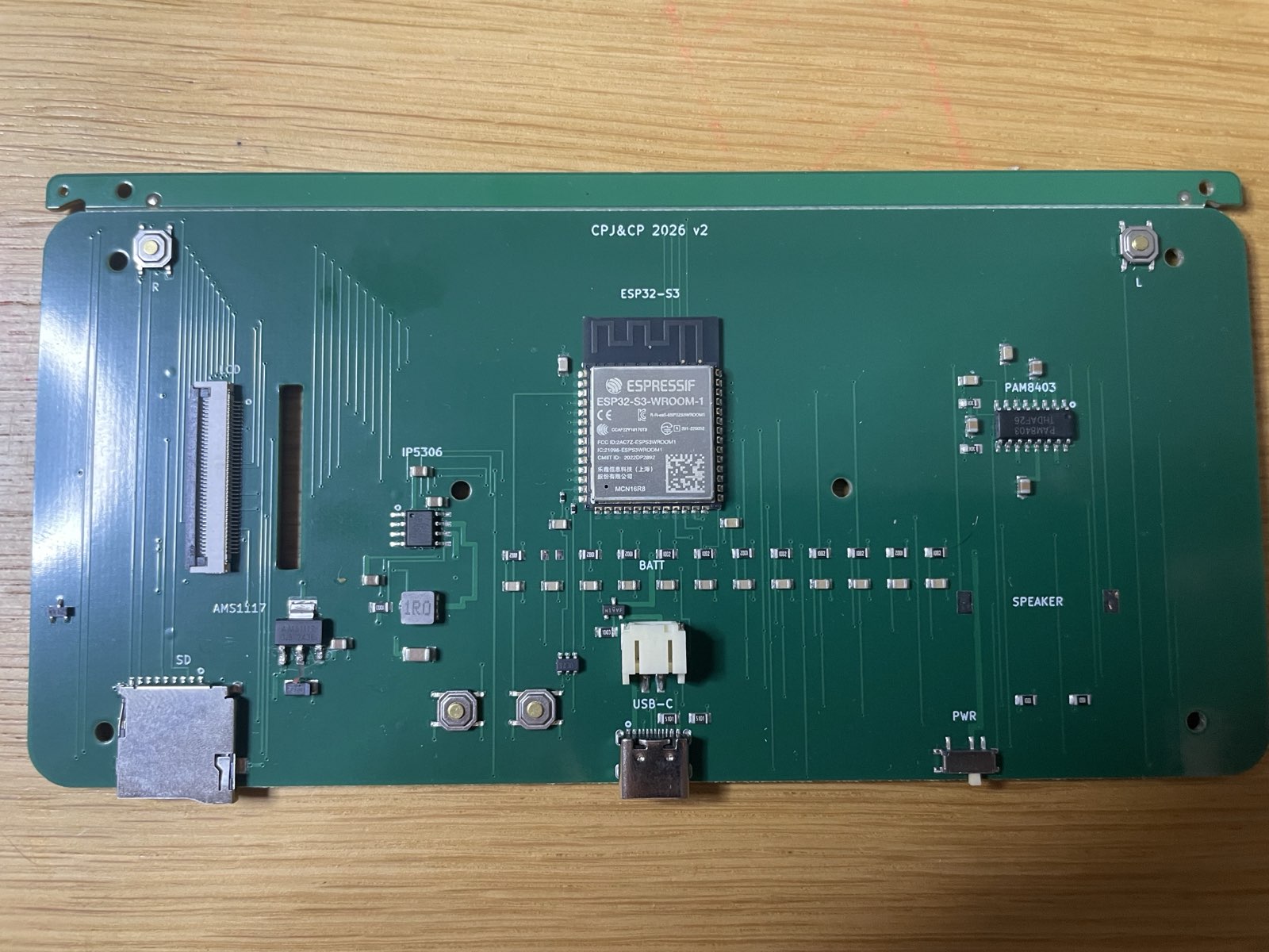
What was found (photo diagnosis, 2026-07-31)
View for all photos and left/right statements: back side, USB-C on the lower edge (mirrored left/right vs. KiCad's un-mirrored bottom rendering).
| Part | Role | Observed | Severity | Consequence |
|---|---|---|---|---|
| U2 IP5306 | charger + 5 V boost | rotated 90°, 0/8 leads on pads | FATAL | no +5V at all |
| U3 AMS1117 | 3.3 V regulator | rotated 90°, leads left instead of down | FATAL | no +3V3 |
| L1 1 µH | boost inductor | marking vertical → rotated | FATAL | boost inoperative |
| Q1 SI2301 | battery reverse-polarity FET | rotated, solder off-pad | FATAL (battery) | no battery power |
| U4 USBLC6 | USB ESD protection | rotated 90°, 0/6 leads on pads | SEVERE | no ESD, USB data at risk |
| C2 22 µF tant. | +3V3 bulk / LDO stability | reversed — bench close-up shows 180°, stripe on GND (own incident) | SEVERE | +3V3 hard short, kills regulators |
| C1 + other MLCCs | decoupling | some 0805s vertical on horizontal pads | DEGRADED | noisy rails |
| D1 BAT54C | START+SELECT→MENU combo diode | rotated, crooked | MINOR | MENU combo dead |
| U5 PAM8403, ESP32 module, top side | — | correctly mounted | OK | — |
Note the survivors: U5, the ESP32-S3 module, both LEDs and the whole top side. The error was selective — exactly the parts whose CPL rotations the July audit later corrected — which rules out a photography/orientation artifact.


How the diagnosis was verified (no bench instruments)
Four independent checks, so no single convention could poison the verdict:
- Photo frame. Back side, USB-C down; confirmed by three placement anchors (AMS1117, IP5306, PAM8403 appear where the mirrored geometry predicts).
- Fabricated copper.
release_jlcpcb/at v4.3.1 — the origin of the ordered gerbers — is identical to the design file for every part listed, so the physical pad geometry is known exactly. - Datasheet pinouts (LCSC): IP5306 1=VIN, 5=KEY, 6=BAT, 7=SW, 8=VOUT, EP=GND · AMS1117 1=GND, 2+tab=VOUT, 3=VIN · SI2301 G/S/D · BAT54C A/A/K · USBLC6 1/3/4/6=I/O, 2=GND, 5=VBUS. Every pad on the board carries exactly the net the datasheet requires → the design is right; the placement is wrong.
- Witness traces. For each pad, the direction its trace arrives from was
extracted from the release PCB and matched against the photos. Example: the
thin
IP5306_KEYtrace exits U2's lower-right pad, drops and staircases left to R16 — clearly visible in the photo under the rotated chip, arriving at pads no chip pin sits on.
A hard lesson inside the lesson: an early read of these photos called U4 "well soldered" because its lead fillets looked clean. Shiny solder is not evidence — body-orientation vs. pad-geometry contradiction is. Judge seating by pads, never by gloss.
Timeline
| Date | Event |
|---|---|
| 2026-04-13 | JLCPCB order SMT026041362110 placed from release_jlcpcb/ |
| 2026-04-15 | dabf830 catches C2 value/polarity + LED2 identity in the pending order (CPL overrides + BOM swap). The C2 incident later shows proto #1 was assembled from pre-fix files — the uploaded order was evidently not refreshed |
| 2026-04-16 | v4.3.1 tagged (audit R23) |
| 2026-07-24 | Bench incident: C2 tantalum reversed on proto #1, +3V3 hard short |
| 2026-07-25/26 | CPL rotation law: U2 / D1 / Q1 rotations corrected by pin→pad→net derivation; 35d6454 also ships the U4 fix that had never reached the release dir |
| 2026-07-31 | Photo diagnosis of the assembled batch: the rotation error was systemic — at least 8 parts, full list above |
Why this cannot happen silently again
verify_cpl_rotation_law+ mutation tests (test_cpl_rotation_law): CPL rotations are derived from one law with declared, justified exceptions — not a hand-maintained table.verify_polarity+hardware/datasheets/POLARITY_AUDIT.md: polarized parts are audited against manufacturer datasheets, not conventions.- The release-dir staleness class (U4's fix sitting unshipped for months) is
the subject of its own rule: every PCB/BOM/CPL commit must update
release_jlcpcb/in the same commit.
Disposition
- Do not fabricate from v4.3.1. No release tag exists after v4.3.1 yet;
cut a new release from current
main(all rotations corrected and gated) before re-ordering. - The assembled v4.3.1 boards are rework references. A full hot-air rework guide (per-part correct orientations with pin→pad→net tables and witness traces) was produced during the diagnosis; the five operations in priority order are: U2+L1 → U3+C2+C1 → Q1 → U4 → D1. With eight parts to rework — one of them an ESOP-8 with a thermal pad — refabrication is the recommended path.
- Instrument-free acceptance test for any reworked or refabricated board: T1 USB only → CHG/FULL LEDs on (both are +3V3 indicators) · T2 battery only, PWR on → same LEDs · T3 USB enumerates and flashes · T4 START+SELECT triggers MENU · T5 display backlight uniform.
Board-level design gaps of the same batch
The datasheet-vs-PCB audit found three design gaps on these boards, separate from the rotation error. They only matter if a board is being revived by rework; all three are fixed in the current design.
1. SD card has no power (critical). The TF-01A slot's pin 4 (VDD) and pin 6 (GND) have no copper. Bodge a 30AWG wire from pin 4 to any +3V3 pad/via and from pin 6 to any GND point; optionally ground two opposite shield pads for EMI. Verify by continuity, then card detection in firmware.
2. PAM8403 application circuit is missing (only if using the speaker). No DC-blocking, bias, or decoupling around U5. Add, all 0805: a 0.47 µF DC-block in series with I2S_DOUT into INR (pin 10 — cut the trace and bridge the cut with the cap), 20 k from INL (7) and INR (10) to VREF (pin 8) — not to GND; the PAM8403 biases its inputs at VREF and grounding them kills the operating point — 100 nF from VREF (8) to PGND, 1 µF from VDD (6), PVDD (4) and PVDD (13) to their grounds. Without a speaker connected the missing passives cause no harm — skip until audio is wanted. Acceptance: clean tone, < 20 mV DC across the speaker.
3. USB-C shield pads undersized (mechanical). Front shield pads are 1.1 mm vs the datasheet's 1.7 mm. Build up generous solder fillets on all four shield tabs (UV-cure adhesive at the base for extra strength); the connector must not move under a firm pull. The current design fixes the pad geometry — see the DFM constraints in the repo.
Shopping list for a full revival: 1× 0.47 µF, 3× 1 µF, 1× 100 nF, 2× 20 k (all 0805) and 30AWG kynar wire.