Electrical Schematics
Complete electrical design for the ESP32 Emu Turbo, split into 6 detailed schematic sheets with cross-sheet global labels.
1. Power Supply
USB-C, IP5306, SY8089 buck, battery
2. MCU
ESP32-S3 + 31 GPIO labels
3. Display
ILI9488 8080 parallel
4. Audio
PAM8403 + speaker
5. SD Card
SPI ROM storage
6. Controls
12 buttons + debounce
USB Data
Native USB — on Sheets 1–2
KiCad 10 project: hardware/kicad/
make generate-schematic   # Generate 7 .kicad_sch files
make render-schematics    # Export SVG + PDF
System Block Diagram
                         ┌──────────────────┐
                         │                  │   +5V_VOUT
    USB-C ──────────────>│   IP5306 Module  │──────────────────┐
                         │  (charge+boost)  │                  │
                         └────────┬─────────┘                  ▼
                                  │ BAT+                ┌────────────┐
                          ┌───────┴───────┐             │ Q2 AO3401A │
                          │ Q1 AO3401A RPP│   gate ────►│ high-side  │
                          ├───────────────┤   SW16 +    │ P-MOSFET   │
                          │ LiPo Batt     │   R32/R33/  └─────┬──────┘
                          │ 3.7V 5000 mAh │   C32 net;        │
                          │ (105080)      │   C33 → KEY       │
                          └───────────────┘   (wake)          │
                                                              │ +5V (loads)
                                          ┌────────────────────┼─────────┐
                                          │                    │         │
                                    ┌─────┴──────┐       PAM8403 (U5)  R27 →
                                    │  SY8089    │       + speaker     backlight
                                    │ 5V -> 3.3V │
                                    └─────┬──────┘
                                          │ 3.3V
                              ┌───────────┴───────────┐
                              │   ESP32-S3-WROOM-1    │
                              │   N16R8 (240MHz ×2)   │
                              └──┬──┬──┬──┬──┬──┬──┬──┘
                                 │  │  │  │  │  │  │
                    ┌────────────┘  │  │  │  │  │  └──────────┐
                    │               │  │  │  │  │             │
              ┌─────┴─────┐  ┌─────┴──┘  │  └──┴─────┐  ┌────┴────┐
              │ Display   │  │ SD Card│  │  │ SPI    │  │ Controls│
              │ ILI9488   │  │ SPI    │  │  │(coproc)│  │ 12 btns │
              │ 8080 ‖    │  └────────┘  │  └───┬────┘  └─────────┘
              └───────────┘              │      │
                                   ┌─────┴──┐  ┌┴─────────────┐
                                   │USB Data│  │ESP32-S3-MINI │
                                   │(D-/D+) │  │  -1 (v2)     │
                                   └────────┘  │  I2S → Audio │
                                               └──────────────┘

  SW16 OFF: Q2 open → all +5V loads dead, USB still charges the cell.
  SW16 ON:  C33 couples a wake pulse into IP5306 KEY, Q2 closes.
Sheet 1 — Power Supply
USB-C input with CC pull-downs, F1 resettable PTC fuse on the VBUS input, IP5306 charge-and-play module, SY8089AAAC synchronous buck regulator (L2 + C30 + R25/R26 feedback divider), Q1 battery reverse-polarity protection, and USBLC6 ESD protection + series resistors on the USB data lines. The respin adds the SW16 power switch network — Q2 high-side P-MOSFET splitting +5V_VOUT from +5V, its gate network (R32/R33/C32/R34) and the IP5306 KEY wake cap C33. It also fits SW17, a do-not-place manual wake button on the KEY node.
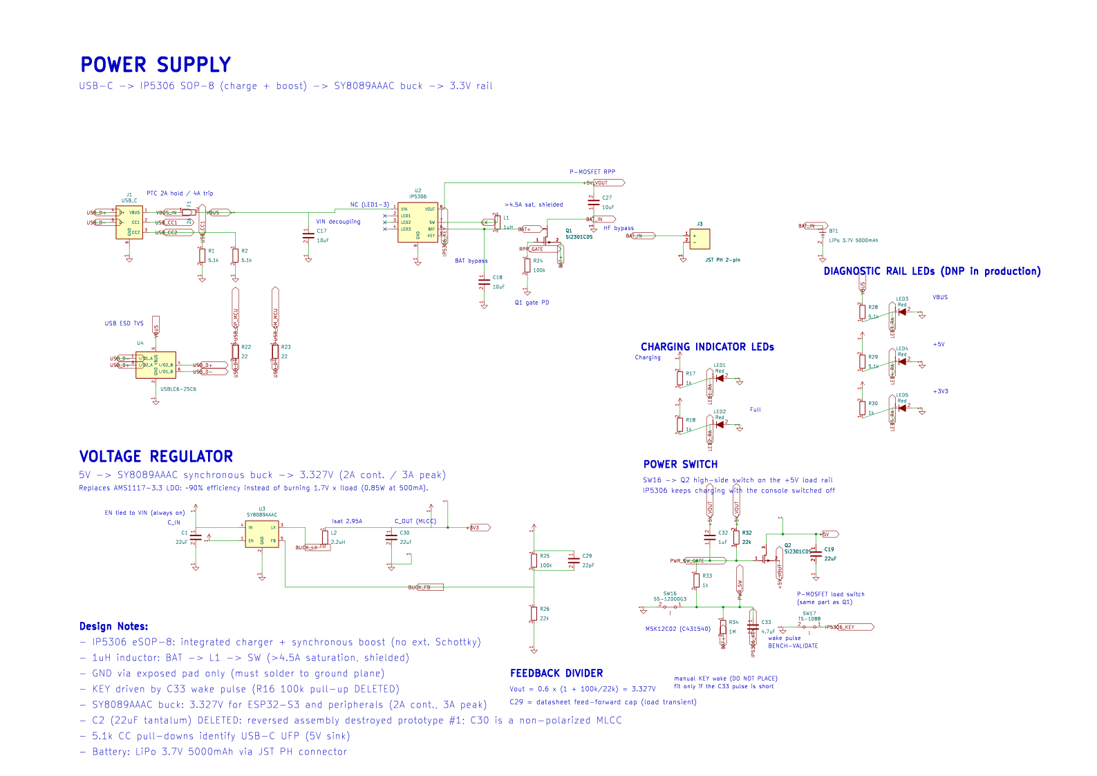
| Ref | Component | Value | Purpose | Datasheet |
|---|---|---|---|---|
| J1 | USB-C connector | — | 5V power input | |
| J3 | JST PH 2-pin SMD connector | C295747 | LiPo battery connector (surface-mount, no through-holes) | PDF — THT sibling C173752; only the mating dimensions apply |
| F1 | PTC resettable fuse | 2 A hold, 1812 (C960026) | VBUS input overcurrent protection: J1 delivers on VBUS_IN, the board's VBUS is reached through F1 (R3-HIGH-4 fix, in design since 1c3ded4) | — |
| R1, R2 | Resistor | 5.1 kΩ | CC1/CC2 pull-down (UFP identification) | |
| Resistor | 100 kΩ | IP5306 KEY pull-UP to +5V — it was never a pull-down, and it was off-datasheet from the start (the IP5306 reference schematic shows KEY with a button to GND and an internal pull-up, no external one). DELETED in the respin; on the new load-side +5V it would invert into a 100 kΩ pull-down whenever the switch is OFF, holding KEY asserted. See the caution below | ||
| R17 | Resistor | 1 kΩ | LED1 current limiting | |
| R18 | Resistor | 1 kΩ | LED2 current limiting | |
| U2 | IP5306 module | — | LiPo charger + 5V boost (charge-and-play) | |
| BT1 | Battery | LiPo 3.7V 5000mAh | 105080 cell | — |
| U3 | Buck regulator | SY8089AAAC | 5V to 3.3V, 2A max, ~93% | |
| U4 | USB ESD TVS | USBLC6-2SC6 SOT-23-6 (C7519) | USB D+/D− ESD protection | — |
| R22, R23 | Resistor | 22 Ω 0402 (C25092) | USB D+/D− series resistors | — |
| Q1 | P-MOSFET | AO3401A SOT-23 (C15127) | Battery reverse-polarity protection (BAT_IN → BAT+). R32: replaced SI2301CDS, rated below the battery-path current | — |
| R24 | Resistor | 100 kΩ | Q1 gate pull-down (MOSFET ON for correct polarity) | |
| Q2 | P-MOSFET | AO3401A SOT-23 (C15127) | Respin — high-side power switch on the +5V rail: source on +5V_VOUT, drain on +5V, gate on PWR_SW_GATE. Same part as Q1. The body diode points loads→VOUT, so it blocks in the OFF state | — |
| R32 | Resistor | 22 kΩ (C17560) | Respin — Q2 gate pull-up, PWR_SW_GATE → +5V_VOUT. Sets the default state to OFF. Not 100 kΩ — see the caution below | — |
| R33 | Resistor | 1 kΩ (C17513) | Respin — series gate resistor, PWR_SW → PWR_SW_GATE; sets the soft-start slope | — |
| R34 | Resistor | 1 MΩ (C17514) | Respin — PWR_SW → BAT+. Defines the switch node when the throw is open and keeps C33 pre-charged | — |
| C32 | Capacitor | 1 µF (C28323) | Respin — Q2 gate-source cap, PWR_SW_GATE → +5V_VOUT: soft-start / inrush limiter, τ = 957 µs. (Not to be confused with C31, which is the ESP32 EN reset cap on Sheet 2 and is untouched) | — |
| C33 | Capacitor | 4.7 µF (C1779) | Respin — wake cap, PWR_SW → IP5306_KEY: AC-couples the switch's ON transition into KEY as a low pulse. Value is BENCH-VALIDATE (sized for the 50 ms–2 s press window, see below) | — |
| SW17 | 2-pad SMD momentary — DO NOT PLACE | C720477 | Respin — IP5306_KEY → GND, the datasheet-blessed manual wake, at (115.15, 56.25) rot 90. In the BOM so it can be sourced, out of the CPL so JLCPCB never fits it. Deliberately not the 5.1×5.1 tact: that footprint has no clearance-legal site in this quadrant | — |
| L1 | Inductor | 1 µH 4.5A | IP5306 boost inductor | |
| LED1 | Red LED | 0805 | Power indicator (+3V3, always on — U2's LED pins are NC on this board) | |
| LED2 | Red LED | 0805 | Second power indicator (+3V3, always on). C19171391 is red (YLED0805R, 615–630 nm) — it was mislabelled "green" in BOM and docs | |
| SW16 | Slide switch | MSK12C02 (C431540) — the held datasheet is MSK12C02, not the SS-12D00G3 it is often called | Power on/off — ⚠ electrically inert in ANY revision to date (v4.4.0 included); the respin gates the +5V loads via a high-side P-MOSFET (Q2) instead, see warning below | |
| L2 | Inductor | 2.2 µH 2.95 A (C36409) | SY8089 buck output inductor | — |
| R25 | Resistor | 100 kΩ | Buck feedback divider, upper leg — Vout = 0.6 × (1 + R25/R26) = 3.327 V | |
| R26 | Resistor | 22 kΩ (C17560) | Buck feedback divider, lower leg | — |
| C29 | Capacitor | 22 pF C0G (C1804) | Feed-forward across R25 (loop phase boost) | — |
| C1 | Capacitor | 22 µF 1206 MLCC | SY8089 buck input decoupling — tight hot loop to VIN/GND | |
| C30 | Capacitor | 22 µF 1206 MLCC | SY8089 buck output — ceramic. (The tantalum C2 that lived here for the AMS1117's ESR window is deleted; it is what destroyed prototype #1, see the incident.) | |
| C17, C18 | Capacitor | 10 µF | IP5306/rail decoupling | |
| C19 | Capacitor | 22 µF | Bulk capacitor on IP5306 VOUT | |
| C27 | Capacitor | 10 µF | IP5306 VOUT HF decoupling — moves to +5V_VOUT in the respin (it stays on the IP5306 side of Q2) |
Datasheet-filename note: shared parts reuse the first reference's
filename, so R16_100k-0805_C149504.pdf is the 100 kΩ 0805 sheet for
R24, R25 and R32 as well. R16 itself is deleted in the respin, so
the filename is now named after a part that no longer exists — it is kept
as-is rather than renamed, because three live references link to it and
the LCSC code (C149504) is what actually identifies the part. Rename it
only together with all three links.
Power Budget
| Consumer | Rail | Typical | Peak |
|---|---|---|---|
| ESP32-S3 (dual-core active) | +3V3 | 150 mA | 350 mA |
| ILI9488 logic + panel drive | +3V3 | 20 mA | 30 mA |
| Backlight (LED-A via R27, always on) | +5V | 90 mA | 95 mA |
| PAM8403 + speaker | +5V | 20 mA | 100 mA |
| SD card (SPI read) | +3V3 | 30 mA | 100 mA |
| Misc (pull-ups, buttons) | +3V3 | 10 mA | 20 mA |
| Total | ~320 mA | ~695 mA |
Battery life: ~12.9 hours typical gameplay.
Not 5000 / 320. That division ignores both conversion stages. The +3V3 rail
(210 mA typical) passes through the SY8089 buck at ~93% (a buck converts
power, so its input current scales by the voltage ratio); the backlight and
PAM8403 draw straight from +5V; and the whole 5V rail is produced by the
IP5306 boosting 3.7V at ~90%:
I_5V  = 210 x 3.3 / (5 x 0.93) + 90 + 20 = 259 mA
I_bat = 259 x 5 / (3.7 x 0.90) = 389 mA   ->  5000 / 389 = 12.9 h
Two design notes baked into these figures: the backlight moved from a hardwired +3V3 tie to +5V through R27 (20 Ω, net LED_BLA, ~90 mA) in the R25 respin — brighter and current-limited, at a real runtime cost — and the SY8089 buck replaced the AMS1117 LDO (a linear regulator draws the full +3V3 current from the 5V rail regardless of output voltage, costing ~25% runtime and ~7x more heat). Fabricated boards through v4.3.1 predate the R27 change and tie LED-A to +3V3.
Power Path Architecture
Topology of the respin (branch respin/sw16-5v-switch). The battery and
USB front ends are unchanged; what is new is that the +5V rail is cut between
the IP5306's VOUT pin and every load by the high-side P-MOSFET Q2:
  MAIN PATH — the switch cuts the load rail only, never the charge path

                          ┌─────────────┐
  USB-C ─VBUS_IN─► F1 ────┤ pin 1 (VIN) │
  (5V)            (PTC)   │             │
                          │   IP5306    │            +5V_VOUT       +5V
                          │    (U2)     │──pin 8──┬────────► Q2 ──────┬──► SY8089 ──► +3V3
  Battery ─BAT_IN─► Q1 ───┤ pin 6 (BAT) │ (VOUT)  │       (PMOS)      │     (U3)   (ESP32, LCD, SD)
  (3.7V)   (J3)   (RPP)   │             │        C27                  ├──► PAM8403 (U5)
                   BAT+   │             │──pin 7 ── L1 ──► BAT+       └──► R27 ──► backlight
                          │             │  (LX)
                          │ pin 5 (KEY) │
                          └───┬─────┬───┘
                            KEY     GND
                              │
  GATE NETWORK — SW16 does nothing but pull PWR_SW to GND

                    +5V_VOUT
                        │
             ┌──────────┴──────────┐
            R32 22k              C32 1µF          default = OFF; C32 = soft start
             │                     │
             └──────────┬──────────┘
                        │
                  PWR_SW_GATE ──────────────────► Q2 gate
                        │
                      R33 1k                      τ = (R32‖R33)·C32 = 957 µs
                        │
      ┌─────────────────┴─────────────────┬──────────────────┐
      │                                   │                  │
   SW16 pad 2                         R34 1M              C33 4.7µF
   (common) = PWR_SW                     │                  │
      pad 1 = GND  ← ON position        BAT+           IP5306_KEY
      pad 3 = OPEN                  (defines the node    (wake pulse
      tabs 4a–4d = mechanical        when the throw       on the ON
      anchors (4b/4d on BTN_SELECT)  is open)             transition)
Key design points:
- Q1 (AO3401A P-MOSFET) sits in series between J3 (net BAT_IN) and the BAT+ rail, with the cell on the drain and the IP5306 on the source. That direction is the protection, not a detail: a P-channel body diode conducts drain→source, so a correctly-inserted cell pre-charges the rail through the diode and then VGS = −VBAT (gate held at GND by R24) turns the channel on, while a reversed cell reverse-biases the diode and holds the channel off. Wired the other way round the part conducts identically in normal use and does nothing at all in the fault — which is why this shipped undetected through v4.5.0 and was fixed as R31-HIGH-1 by turning the package around.
- Q2 (AO3401A P-MOSFET, same part as Q1) is the actual power switch. Its body diode points loads→VOUT, so it blocks in the OFF direction; SW16 does nothing but pull the gate node to GND. Sliding to ON gives VGS = −4.78 V (past the −4.5 V the part's RDS(on) is specified at); the throw open gives VGS = −0.028 V with a cell, −0.108 V with none — against a 0.5 V threshold minimum. vbench T2.3 solves the same network from the netlist and the BOM and gets −4.783 V / −0.025 V.
- The net split follows the board's existing precedent —
VBUS_IN→ F1 →VBUS,BAT_IN→ Q1 →BAT+, and now+5V_VOUT→ Q2 →+5V.+5V_VOUTis the upstream net (U2 pin 8, C27, Q2 source, R32/C32);+5Vkeeps its name and is now the LOAD-side net (U3, U5, R27, load-side decoupling). - SW16 was originally intended between battery and IP5306 pin 6 (BAT) — that plan is rejected, see the caution below. It is not functional in any revision to date, and it never controlled USB VBUS.
- VBUS reaches IP5306 pin 1 (VIN) through the F1 PTC fuse (J1 → VBUS_IN → F1 → VBUS) — always available when USB is plugged in.
- IP5306 passthrough: when USB is connected, VBUS (5V) passes to VOUT regardless of battery state. In the respin that passthrough lands on +5V_VOUT, so Q2 still gates it: USB + switch OFF is a charge-only state, not a run state.
- Charging is upstream of the switch by construction. J3 → Q1 → BAT+ → pin 6 and J1 → F1 → VBUS → pin 1 are untouched, which is exactly why OFF can kill the loads without killing the charger.
- The MSK12C02's contacts are not in series with the rail, and must not be. +5V peaks around 1.5–2 A (buck plus PAM8403), well above what a slide switch of this class is rated to break; through the gate divider the contacts carry 217 µA. That is the second reason the switch drives a gate rather than the current — the first being that a switch in the cell path would break charging.
- Consequence for debug workflows: OFF no longer means "system on USB with the battery isolated". With USB plugged in and SW16 OFF the board only charges — serial and flash need SW16 ON. Battery isolation for bench work is still "unplug J3".
- No backfeed diode needed: IP5306 charger is internally regulated (CC/CV), boost is unidirectional.
In every revision to date (v4.4.0 included), PCB routing connects only the switch
common pin (2) to BAT+ as a dead stub; throw pins 1/3 are unrouted
(hardware/datasheet_specs.py declares them unconnected). The battery path
J3 → Q1 → BAT+ → IP5306 pin 6 is continuous copper that never passes through the
switch, so sliding it changes nothing. Consequences on those boards:
- Every power-state row below behaves as its SW16 = ON row, whatever the switch is set to.
- To truly isolate the battery (e.g. for flashing), unplug the J3 battery connector.
- There is no on/off mechanism at all.
IP5306_KEY = {R16.2, U2.5}— a static 100 kΩ pull-up to +5V and no button — so the only thing that ever cuts VOUT is the IP5306's automatic light-load standby, which cannot then be woken except by plugging USB in. (The older claim here, "system on/off relies on the IP5306 KEY logic (SW13/MENU via R16)", was false: SW13 is the menu button and sits onMENU_K→ D1 →BTN_START/BTN_SELECT; it has nothing to do with KEY.)
Required behaviour (user spec, decided 2026-08-03) — SW16 ON: everything powered, from the battery boost or from USB passthrough. SW16 OFF: all loads dead, but USB still charges the battery. No battery installed: identical, with USB passthrough powering the loads when ON.
Putting the battery in series with the switch is REJECTED. That was the plan recorded here for months, and it fails for two independent reasons: (1) OFF would break the charge path too, so the board could not charge with the switch off; (2) with USB plugged in, the IP5306's VBUS→VOUT passthrough keeps the system running regardless of the battery terminal, so a battery-side switch does not actually switch the system off.
Implemented instead (branch respin/sw16-5v-switch, full derivation in the RESPIN
section of
docs/known-issues.md):
the +5V rail is broken between the IP5306 VOUT pin and all loads by the high-side
P-MOSFET Q2 (AO3401A, same part as Q1). New net +5V_VOUT upstream, +5V keeps
its name on the load side. SW16 pad 2 = PWR_SW, pad 1 = GND (the ON position),
pad 3 open; the dead BAT+ stub is removed. Gate network: R32 22 kΩ pull-up to
+5V_VOUT (default OFF), R33 1 kΩ in series, C32 1 µF gate-source
(soft start, τ = 957 µs → ~1.5 ms ramp → ~167 mA inrush instead of amps), R34
1 MΩ from PWR_SW to BAT+.
R32 is not 100 kΩ. The OFF state is a divider — VGS = −5 × R32/(R32+R33+R34) — so the gate offset is set by the ratio, and the obvious 100k/10k/1M lands the no-battery case on VGS = −0.455 V, exactly the P-MOSFET's threshold-minimum region, in precisely the USB-powered/no-cell/switch-OFF state a bench operator uses most. Raising R34 to 4.7 MΩ fixes the same ratio and was rejected for a different reason: 4.7 M 0805 is not a JLCPCB Basic part, so it would buy an extended-part fee and a feeder. Shrinking R32 uses parts already on this BOM, keeps R34 on the Basic 1 M, and is better electrically twice over — a 23 kΩ gate network is far harder to disturb than a 110 kΩ one, and the ON-state divider improves from −4.55 V to −4.78 V. C32 grew to 1 µF for the same reason: at 957 Ω a 100 nF cap gives τ = 96 µs, and a 96 µs ramp puts about 1.7 A through Q2. The time constant is the specification, not the capacitor value.
The wake network is mandatory, not polish. The IP5306 boost auto-shuts down after
32 s below a 45 mA load and restarts only on a KEY press or a USB insertion
(datasheet V1.32 §10/§12). With SW16 OFF the load behind Q2 is ~0.1 mA, so the boost
will latch off every time — and flipping back to ON must therefore generate a KEY
press by itself, or the board never comes back on battery. C33 (4.7 µF from PWR_SW
into IP5306_KEY) couples the ON transition into KEY as a low pulse; KEY is active-low
with an internal pull-up per the datasheet reference schematic (p.11, fig. 4), and the
chip stays alive from the cell while the boost is off. The pulse width is τ against
that undocumented internal pull-up, so the C33 value is BENCH-VALIDATE. Sizing:
the chip accepts a press of 50 ms–2 s (shorter is ignored; longer is a "long press",
which does not start the boost), and the synthesized press lasts ≈ 0.7 τ — so
4.7 µF is safe for an internal pull-up anywhere in ≈ 15 kΩ–600 kΩ, where the first-cut
1 µF needed ≥ ≈ 70 kΩ to register at all. Community practice (driving KEY low through
1–1.2 kΩ for ~100 ms as the standard auto-shutdown workaround) confirms the press model.
SW17 is the fallback and the tuning point. It is a 2-terminal SMD momentary
(C720477) at (115.15, 56.25) rot 90, 3.9 mm from C33.2 — which is the KEY node —
marked DO NOT PLACE: the land and copper are on the board, the part is in the BOM
so it can be sourced, and it is absent from the CPL so JLCPCB never fits it. It is
deliberately not the 5.1 × 5.1 tact the user buttons use: a 7.0 × 4.4 footprint
has no clearance-legal site anywhere in the IP5306 quadrant, even with every respin
part and every piece of respin copper treated as movable — the only sites are north
of U2, past the BAT+ B.Cu run at y = 46.1, and the one F.Cu corridor across it is
0.925 mm wide and already carries PWR_SW. There is no series resistor in the
KEY leg: C33's 4.7 µF already dominates that node's impedance, and an R would sit in
the wake pulse's own path.
R16 is deleted — it was off-datasheet from the start, and on the new load-side +5V
it would invert into a 100 kΩ pull-down whenever the switch is OFF, holding KEY
asserted. IP5306_KEY becomes {U2.5, C33}.
Power States & Debug
These rows describe the respin topology (Q2 gating the +5V loads). On every board fabricated to date the switch is inert, so every state behaves as its SW16 = ON row — see the caution above.
| # | USB | SW16 | Reset | Boot | +3V3 | ESP32 | Charging | Serial | Flash |
|---|---|---|---|---|---|---|---|---|---|
| 1 | No | OFF | — | — | OFF | OFF | No | No | No |
| 2 | No | ON | — | — | ON | Run | No | No | No |
| 3 | No | ON | Press | — | ON→OFF→ON | Reset | No | No | No |
| 4 | Yes | OFF | — | — | OFF | OFF | Yes | No | No |
| 5 | Yes | ON | — | — | ON | Run | Yes | Yes | No |
| 6 | Yes | ON | Press | Hold | ON→OFF→ON | DL mode | Yes | No | Yes |
State legend:
- #1: everything dead. Q2 is open and there is no source; the board draws ~0.1 mA of leakage through the gate network.
- #4 is charge-only — the switch cuts only the +5V loads. VIN → BAT charging is upstream of Q2 and stays intact, so the cell charges with the whole system powered down. There is no serial and no flashing here: the ESP32 has no rail.
- #5 and #6 require SW16 ON. Serial, flashing and download mode all need the ESP32 powered, and on a respin board that means the switch is ON.
- #5: charge-and-play — the IP5306 charges the battery AND powers the system simultaneously.
- DL mode: ESP32 download mode (hold BOOT, press+release RST, release BOOT).
- The switch is not battery isolation. Q2 opens the load rail, not the cell; true battery isolation is still unplugging J3.
- With no battery fitted the rows are identical, with Charging read as "—":
USB passthrough feeds
+5V_VOUT, and Q2 decides whether it reaches the loads.
Flash & Debug Procedures
Flash firmware (switch ON):
- Connect USB-C cable
- Set SW16 to ON. On a respin board OFF cuts the +5V loads, so the ESP32 has no rail and cannot be flashed at all; on every board built to date both positions work because the switch is inert. For true battery isolation during flashing, unplug J3 — the switch never does that.
- Hold SW14, press+release SW15, release SW14
- Run
idf.py flash— ESP32 enters download mode - Press SW15 to reboot into normal mode
Serial debug monitor:
- Connect USB-C cable, SW16 ON (on boards built to date either position works — the switch is inert)
- Run
idf.py monitor(115200 baud via USB CDC on GPIO19/20) - Press SW15 to restart — monitor auto-reconnects
Charge-and-play:
- Connect USB-C with SW16 ON
- System runs normally while battery charges
- LED1 and LED2: both red, both plain +3V3 power indicators. The old "LED1 = charging, LED2 (green) = fully charged" description was aspirational — the IP5306's LED pins (2–4) are NC on the fabricated board, and C19171391 is a red part despite its BOM label. Respin: route U2 pins 2/4 to the LEDs if charge indication is wanted
Backfeed Protection Analysis
| Path | Protection | Mechanism |
|---|---|---|
| VBUS → BAT+ | IP5306 internal charger | CC/CV regulated, max 1A |
| BAT+ → VBUS | Boost unidirectional | IP5306 boost only drives BAT→VOUT |
| USB + switch OFF | Charge-only (respin) | Q2 opens the +5V loads, so nothing downstream is powered; VIN → BAT charging is upstream of Q2 and untouched, so the cell still charges. This is not battery isolation — for that, unplug J3. On boards built to date the switch is inert and this row behaves as the one below |
| USB + switch ON | Charge-and-play | IP5306 manages both paths internally |
| Reversed battery | Q1 P-MOSFET RPP | Cell on the drain: the body diode is reverse-biased and the R24 gate pull-down leaves VGS positive, so channel and diode both block |
Sheet 2 — MCU (ESP32-S3)
ESP32-S3-WROOM-1 N16R8 with all 31 GPIO connections grouped by function, decoupling capacitors, and the EN reset RC network (R3 + C31, added in the R25 respin). LCD_RD is hardwired to +3V3 on the PCB and the backlight is fed from +5V via R27 (neither is GPIO-controlled).
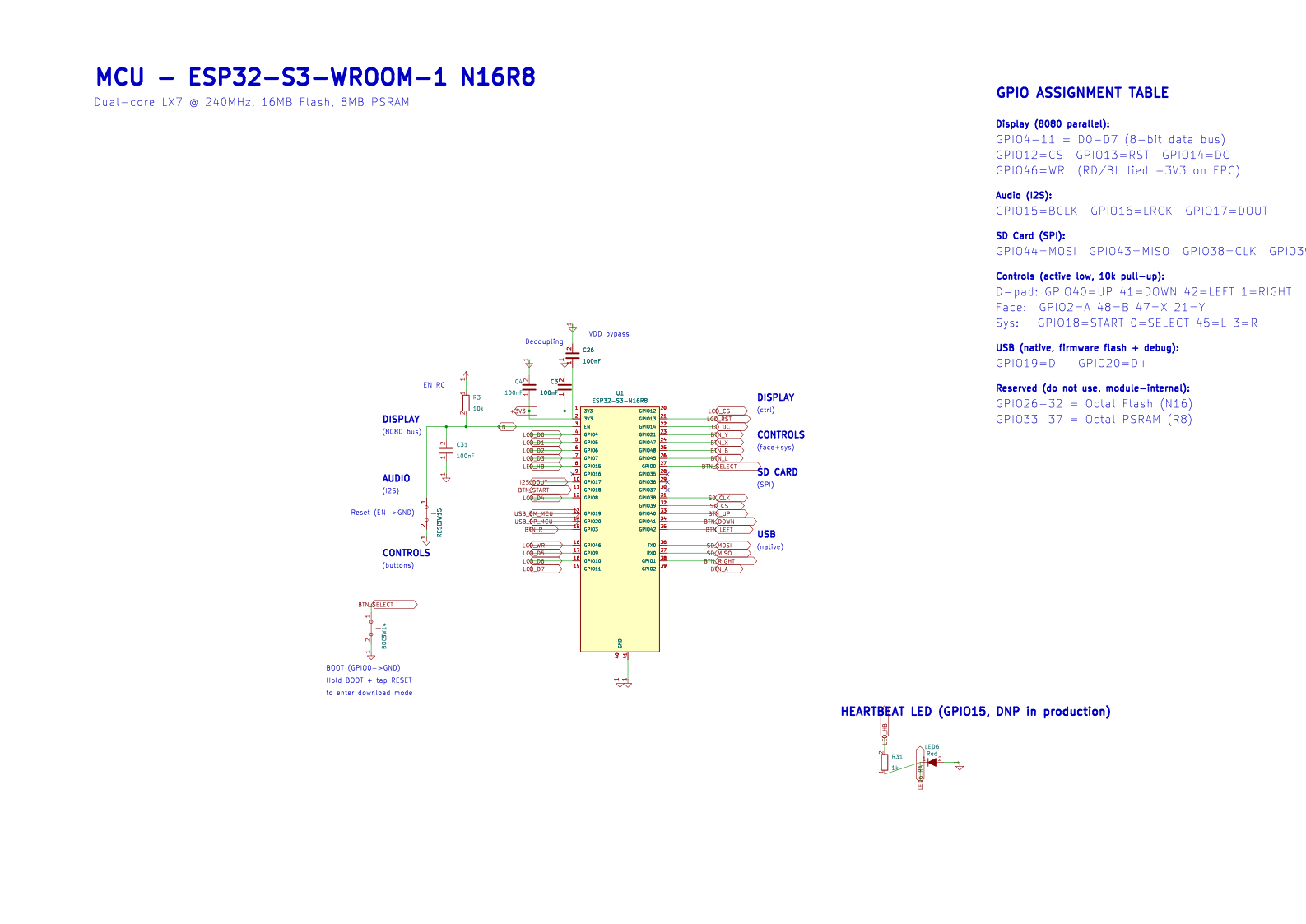
| Ref | Component | Value | Purpose | Datasheet |
|---|---|---|---|---|
| U1 | MCU module | ESP32-S3-WROOM-1 N16R8 | 16MB Flash, 8MB PSRAM | |
| R3 | Resistor | 10 kΩ | EN pull-up to +3V3 (R25 respin, 1c3ded4 — the earlier "WROOM-1 integrates an EN pull-up" claim was falsified: the module has none, and boards through v4.3.1 shipped without any RC) | |
| C31 | Capacitor | 100 nF | EN → GND reset delay (RC ≈ 1 ms with R3, module datasheet p.28 power-up timing) | |
| C3 | Capacitor | 100 nF | 3V3 decoupling (twin of C4) — NOT the EN cap; that is C31 | |
| C4 | Capacitor | 100 nF | 3V3 decoupling | |
| C26 | Capacitor | 100 nF | 3V3 VDD bypass (within 3.6 mm of module pin 2) | |
| SW15 | Tact switch | — | EN reset (pulls EN low) | |
| SW14 | Tact switch | — | Boot mode (pulls GPIO0 low) |
GPIO Assignment
| Function | GPIOs | Signals | Bus |
|---|---|---|---|
| Display | 4–11 | D0–D7 | 8080 data |
| 12, 13, 14, 46 | CS, RST, DC, WR | 8080 control | |
| — | RD | Tied to +3V3 (hardwired) | |
| — | BL | +5V via R27 20 Ω (net LED_BLA, always on) | |
| Audio | 17 | I2S_DOUT | PDM TX (single pin — no BCLK/LRCK) |
| 15, 16 | — | Unconnected: the I2S clock reservation was retired with the move to PDM | |
| SD Card | 44, 43, 38, 39 | MOSI, MISO, CLK, CS | SPI |
| D-pad | 40, 41, 42, 1 | UP, DOWN, LEFT, RIGHT | GPIO |
| Face | 2, 48, 47, 21 | A, B, X, Y | GPIO |
| System | 18, 0 | START, SELECT | GPIO |
| Shoulder | 45, 3 | L, R | GPIO |
| USB Data | 19, 20 | USB_D-, USB_D+ | USB |
GPIO26–32 are the WROOM-1's internal SPI flash bus and are not brought out on any module pin. GPIO33–37 belong to the N16R8's Octal PSRAM — GPIO35–37 do appear on module pins 28–30 but carry explicit no-connect markers in the schematic and must stay unconnected. GPIO19/20 are the native USB D-/D+ pins (firmware flash + debug console via USB CDC).
Sheet 3 — Display
ILI9488 3.95" 320×480 bare panel with 40-pin FPC, 8-bit 8080 parallel interface — mandatory for SNES emulation speed. FPC pin mapping per ILI9488 panel datasheet: pins 9-12=CS/DC/WR/RD, pin 15=RESET, pins 17-24=DB0-DB7, pin 33=LED-A (backlight — fed from +5V through R27 on net LED_BLA, ~90 mA, always on), pins 6-7=VDDI/VDDA(+3V3), pins 38-39=IM0/IM1(+3V3), pin 40=IM2(GND). Note: on the PCB, display Pin N maps to connector Pad (41−N) due to the landscape FPC pass-through (see PCB docs).
| Ref | Component | Value | Purpose | Datasheet |
|---|---|---|---|---|
| J4 | FPC connector | 40-pin 0.5mm bottom contact | Display ribbon cable | |
| R27 | Resistor | 20 Ω 1206 | Backlight series resistor: +5V → R27 → LED_BLA → FPC pad 8 (panel pin 33, LED-A). R25-HIGH-1 fix, in design since 1c3ded4; boards through v4.3.1 tie LED-A to +3V3 instead | — |
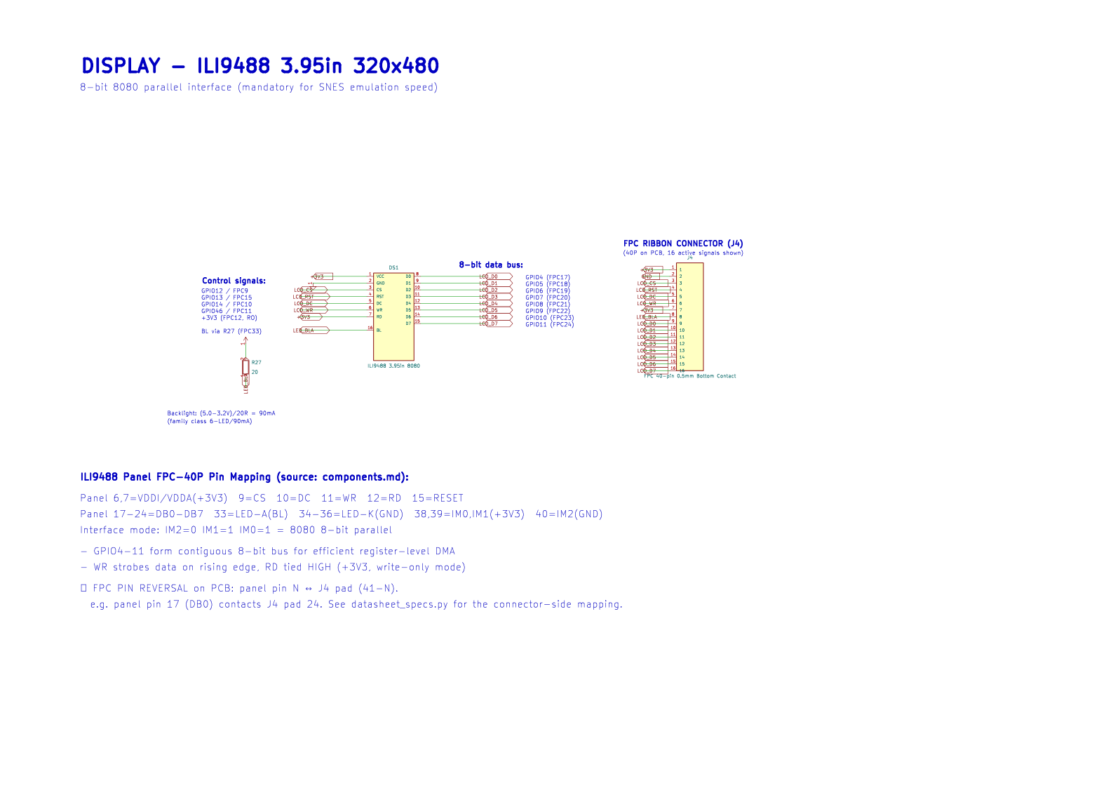
The 8080 parallel mode writes a full pixel (16-bit RGB565) in 2 bus cycles. SPI would need 16 clock cycles per pixel, making it too slow for 60fps full-screen SNES rendering. GPIO4–11 form a contiguous 8-bit data bus for efficient register-level DMA.
Sheet 4 — Audio
I2S output from ESP32-S3 to PAM8403 Class-D amplifier driving a 28mm 8Ω speaker.
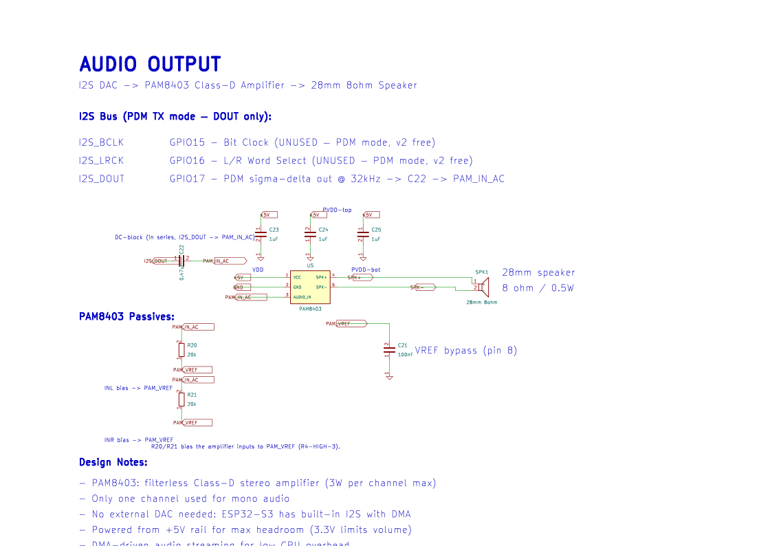
| Ref | Component | Value | Purpose | Datasheet |
|---|---|---|---|---|
| U5 | Amplifier | PAM8403 | Filterless Class-D, 3W/ch | |
| C21 | Capacitor | 100 nF (C49678) | VREF bypass capacitor | |
| C22 | Capacitor | 0.47 µF (C13967) | DC-blocking cap on audio input | — |
| C23, C24, C25 | Capacitor | 1 µF (C28323) | VDD and PVDD decoupling caps | — |
| R20, R21 | Resistor | 20 kΩ (C4328) | Bias resistors on INL/INR to VREF (pin 8), not GND | — |
| LS1 | Speaker | 28mm 8Ω 0.5W | Mono output | — |
The PAM8403 is powered from the +5V rail for maximum headroom. Only one channel is used for mono audio. ESP32-S3 I2S with DMA provides low-CPU-overhead audio streaming. The passive components (C21–C25, R20–R21) follow the PAM8403 datasheet application circuit for proper biasing, DC blocking, and power supply decoupling.
Sheet 5 — SD Card
Micro SD card module via SPI bus for ROM storage (SNES ROMs up to 6MB, FAT32).
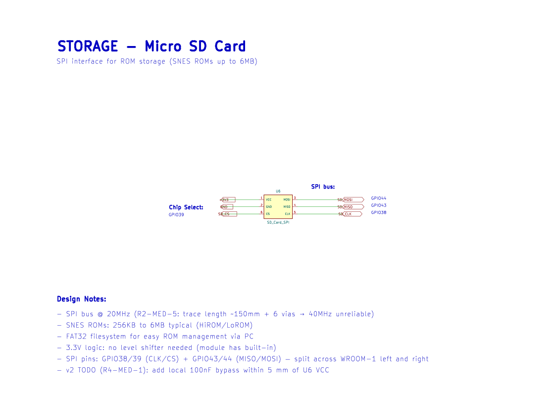
| Ref | Component | Datasheet |
|---|---|---|
| U6 | Micro SD slot (TF-01A) |
| Signal | GPIO | Direction |
|---|---|---|
| MOSI | GPIO44 | ESP32 → SD |
| MISO | GPIO43 | SD → ESP32 |
| CLK | GPIO38 | ESP32 → SD |
| CS | GPIO39 | ESP32 → SD |
SPI bus up to 20MHz. The SD module has a built-in level shifter (3.3V safe). On the PCB, the SD card slot VCC and GND pins are connected via vias to the inner power planes (+3V3 and GND) for clean power delivery with minimal trace length.
Sheet 6 — Controls
13 tact switches (SNES layout + MENU) with individual 10kΩ pull-up + 100nF debounce per button. Plus SW15 (reset) and SW14 (boot mode) on Sheet 2. Tact switch datasheet: PDF.
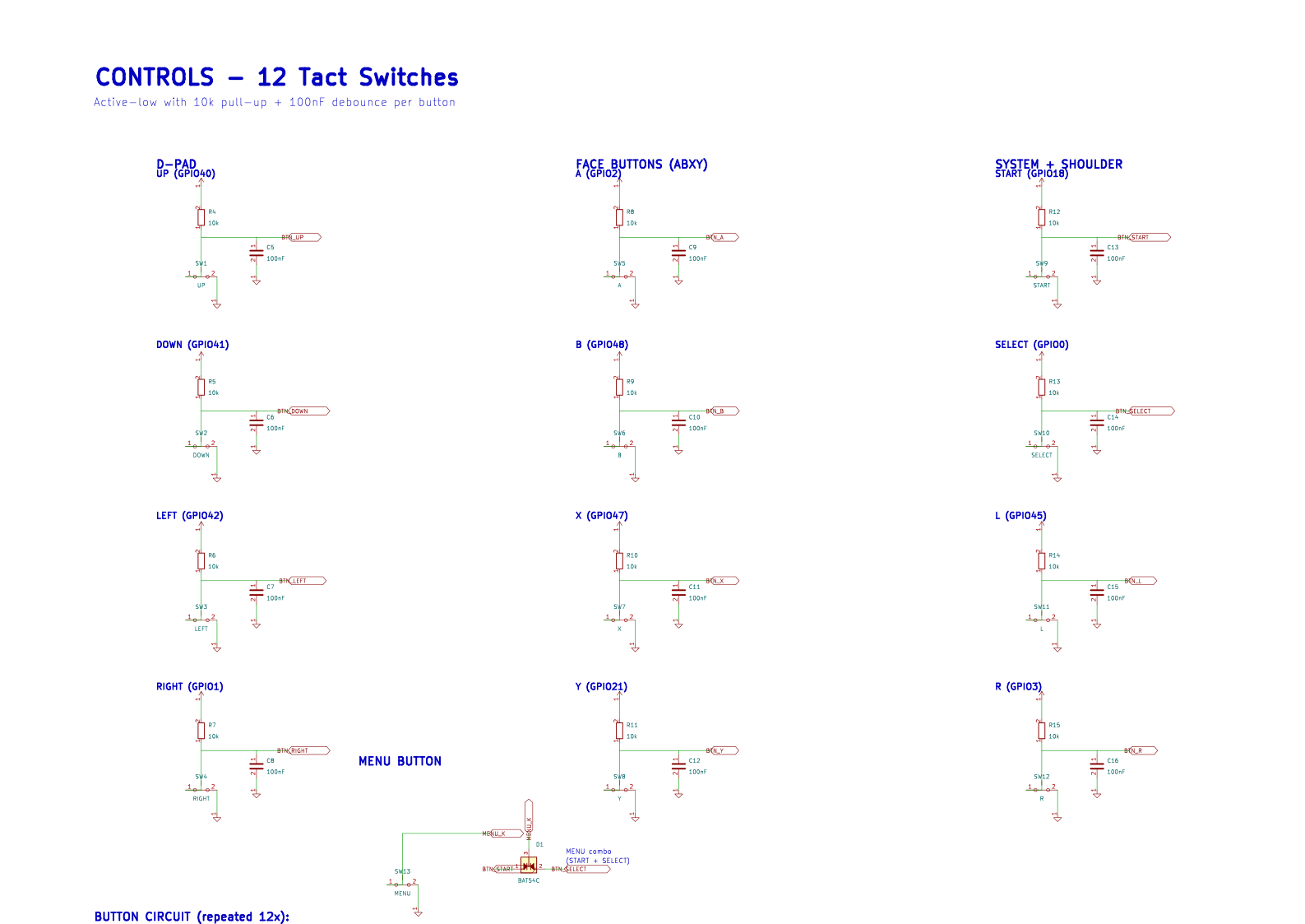
Button Circuit (repeated 13×)
+3V3 ──[10kΩ R]──┬──── GPIO_x (global label)
                  │
                [100nF C]
                  │
                 GND

     [SW tact]──┤
                └── GND
Idle = HIGH (3.3V via pull-up), Pressed = LOW (grounded through switch).
| Ref | Component | Value | Purpose |
|---|---|---|---|
| R4–R13, R15 | Resistor | 10 kΩ (C17414) | Button pull-ups — 11 of the 12 buttons |
| R14 | Resistor | DNP | BTN_L (GPIO45) gets no external pull-up: GPIO45 is the VDD_SPI strapping pin, and a pull-up would force VDD_SPI to 1.8 V and break the Octal PSRAM. Firmware enables the internal pull-up after boot |
| C5–C16 | Capacitor | 100 nF (C49678) | Button debounce (12 buttons) |
| Group | Buttons | Switches | GPIOs |
|---|---|---|---|
| D-pad | UP, DOWN, LEFT, RIGHT | SW1–SW4 | 40, 41, 42, 1 |
| Face | A, B, X, Y | SW5–SW8 | 2, 48, 47, 21 |
| System | START, SELECT, MENU | SW9, SW10, SW13 | 18, 0, — |
| Shoulder | L, R | SW11, SW12 | 45, 3 |
USB Data (flash & debug)
Native USB data lines for firmware flashing and debug console (replaces UART debug).
There is no dedicated sheet: the USB data path is drawn on Sheet 1 (J1 → U4 USBLC6
ESD protection → R22/R23 22 Ω series resistors) and lands on Sheet 2 at ESP32
GPIO19/20 via the USB_D-/USB_D+ global labels.
| Signal | GPIO | Function |
|---|---|---|
| USB_D- | GPIO19 | USB data minus (native USB) |
| USB_D+ | GPIO20 | USB data plus (native USB) |
USB-C now carries both power (charging via IP5306) and data (firmware flash + CDC debug console). This replaces the previous UART debug approach (GPIO43 TX0) with native USB, which is faster and requires no external UART adapter. See Power States & Debug for the full operating modes table and flash/debug procedures.
The optional PSP joystick (previously GPIO20/GPIO44) has been removed. The D-pad provides full SNES/NES control. GPIO43 (previously TX0 for UART debug) is now used for SD_MISO. BTN_R is on GPIO3.
v2 — additional sheet: Audio Coprocessor (ESP32-S3-MINI-1)
"v2" on this page means the planned audio-coprocessor respin, which no fabricated or tagged revision implements yet: every release tag so far (v4.0 → v4.4.0) is a revision of the single-MCU board this document calls "v1". The current board uses direct I2S from the main ESP32-S3 to the PAM8403 (Sheet 4). In the coprocessor revision, the main ESP32-S3 communicates with the coprocessor via SPI, and the coprocessor drives I2S to the PAM8403.
ESP32-S3-MINI-1-N8 audio coprocessor with SPI slave interface to the main ESP32-S3 and I2S output to the PAM8403 amplifier.
| Ref | Component | Value | Purpose |
|---|---|---|---|
| U7 | ESP32-S3-MINI-1-N8 | Module | Audio coprocessor (SPC700 + I2S) |
| C34 | Capacitor | 100 nF | 3V3 decoupling |
| C35 | Capacitor | 100 nF | EN decoupling |
(References C1–C33 are all taken on the v1 board — C28 is a DNP placeholder, C29 is the buck feed-forward, C30 the buck output, C31 the EN reset cap, and C32/C33 are the SW16 respin's gate and wake caps — so the coprocessor starts at C34.)
SPI Bus (Main ESP32-S3 → Coprocessor)
| Signal | Main ESP32-S3 GPIO | MINI-1 GPIO | Direction |
|---|---|---|---|
| SPI_CLK | GPIO 15 (unused in v1) | GPIO 12 | Main → MINI-1 |
| SPI_MOSI | GPIO 16 (unused in v1) | GPIO 11 | Main → MINI-1 |
| SPI_MISO | GPIO 17 (was I2S_DOUT) | GPIO 13 | MINI-1 → Main |
| SPI_CS | GPIO 20 (was USB_D+) | GPIO 10 | Main → MINI-1 |
I2S Bus (Coprocessor → PAM8403)
| Signal | MINI-1 GPIO | Direction |
|---|---|---|
| I2S_BCLK | GPIO 15 | MINI-1 → PAM8403 |
| I2S_LRCLK | GPIO 16 | MINI-1 → PAM8403 |
| I2S_DOUT | GPIO 17 | MINI-1 → PAM8403 |
v2 GPIO Changes vs v1
| Main ESP32-S3 GPIO | v1 Function | v2 Function | Notes |
|---|---|---|---|
| GPIO 15 | unconnected (PDM needs no BCLK) | SPI_CLK → MINI-1 | Spare pin put to work |
| GPIO 16 | unconnected (PDM needs no LRCK) | SPI_MOSI → MINI-1 | Spare pin put to work |
| GPIO 17 | I2S_DOUT → PAM8403 | SPI_MISO ← MINI-1 | Audio path moves to coprocessor |
| GPIO 20 | USB_D+ (native USB) | SPI_CS → MINI-1 | USB D+ reassigned for coprocessor |
GPIO 15/16 (already spare in v1) plus the single PDM pin GPIO 17 freed by moving audio to the coprocessor become the SPI link — no GPIOs wasted. GPIO 20 (USB_D+ in v1) is reassigned to SPI chip select; in v2, USB native data is no longer available (debug via SPI or UART instead).